
Modeling the layout of RF switches
Introduction
It is well known that compact wireless devices require small antennas whose size is dictated mostly by mechanical, design and aesthetic aspects, and not so much on the efficiency of radiation. Therefore, such small antennas are often made tunable to cater for multiband requirements. To make an antenna tunable, a switch is often incorporated to the antenna radiator. Such a device is also called an aperture-tuned antenna.
Although a typical RF switch is a small component, its layout can have an effect on the operation of the wireless system, especially at higher frequencies. If layout effects (e.g. connecting traces) are not accounted for, simulation results do not always match well with reality. As layout effects introduce complicated interconnections, a combined study of an antenna, a switch and an element representing the layout has been challenging, even with previous versions of Optenni Lab. But not anymore with Optenni Lab version 6.0, introduced in fall 2023!
Optenni Lab’s New Schematic Entry Feature
With Optenni Lab 6.0 and its Schematic Entry mode we can approach the switch+layout design problem with (at least) three methods, named as follows:
- Method 1 “No layout”: Antenna and switch are separate blocks wired together, and the layout aspects are simply not accounted for.
- Method 2 “Separated”: Layout aspects are separated into a separate layout representation which is wired to the antenna and switch. In other words, antenna, switch and switch layout model are separate elements.
- Method 3 “Combined”: Antenna and switch layout are represented in the same element, wired to the switch.
Method 1 – No layout
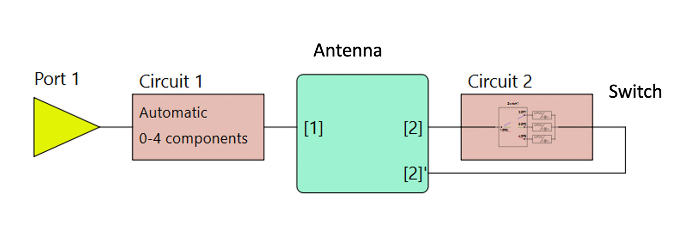
In this case antenna is assumed to have Port 1 as input feeding port with a static matching circuit (to be synthesized), and Port 2 (2-2’) as a component port. The switch is placed in the component port and has no layout information. The antenna is represented as a 2-port impedance data block and the corresponding efficiency and radiation pattern data for each port, coming from a 3D EM antenna simulation. This model simply neglects the effect of the layout of the switch. In other words, the model assumes that the switch and its interconnections have a zero or negligible electrical length (size). If this is not true, this model runs into difficulties.
Method 2 – Separated
An example of Method 2 with a separated antenna, switch and a switch layout model is given in the following.
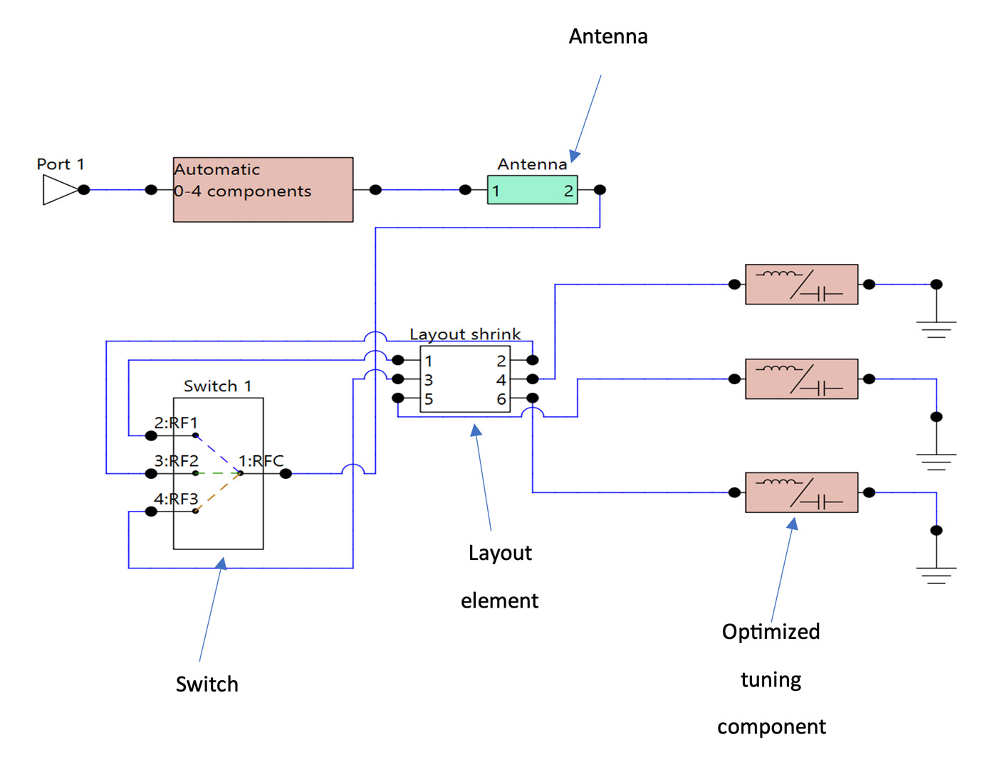
Antenna is connected similarly to the switch as in Method 1. The switch throw ports RF1-RF3 are connected to a layout element simulated in a 3D EM model. The layout element connects also the tuning components to be chosen and optimized by Generic Reactances. In this case, the antenna block is aware of radiation aspects (e.g. radiation pattern, efficiency), whereas the layout element is not – only the six-port impedance data of the layout block is used. Thus, this approach is applicable if it is assumed that the radiation and coupling of the switch layout model to the antenna can be neglected.
Method 3 – Combined
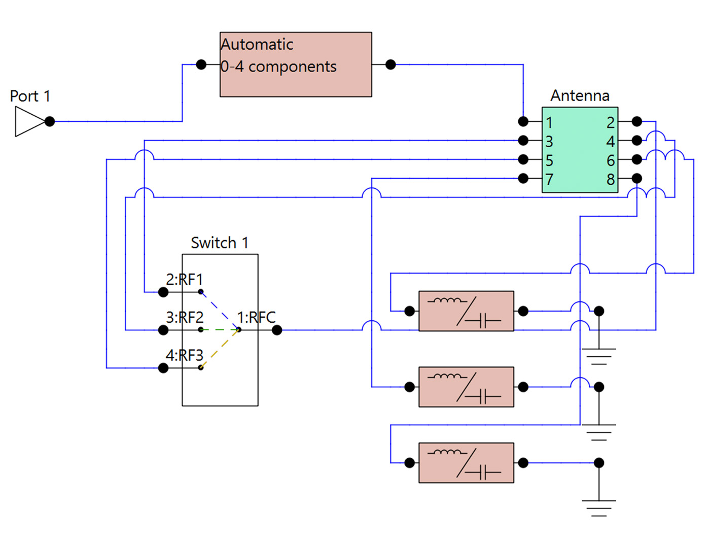
Here both the antenna and the switch layout are combined in a single antenna element in a 3D EM simulation. Thus, the switch throw ports RF1-RF3 are directly connected to the antenna block which is also connected to the optimized tuning components.
In this case, the antenna element captures the “full” electromagnetic behavior of both the antenna radiator and the layout. It takes into account any possible couplings between the antenna the layout, and also accounts for any losses due to radiation from the layout’s interconnections.
However, this method is most challenging in terms of the 3D EM analysis, e.g. involving possible accumulated error due to a very large number of mesh elements and very detailed discretization in details of both antenna’s and layout’s surroundings etc. Therefore, it is not certain that this method yields the most accurate solution with 3D EM simulations.
What is the Effect of the Layout?
We synthesized a matching circuit for 3 bands using Method 1. In the following, let’s compare the results of Method 3 with the results obtained when synthesized component values of Method 1 are inserted into Method 3.
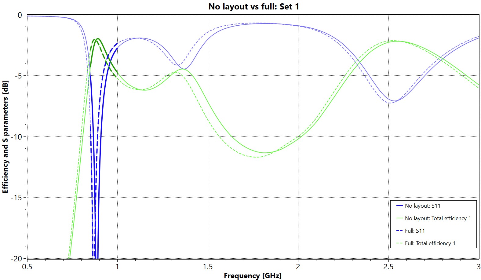
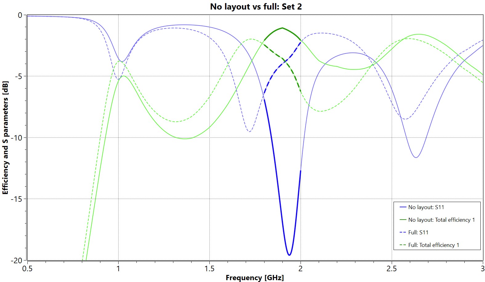
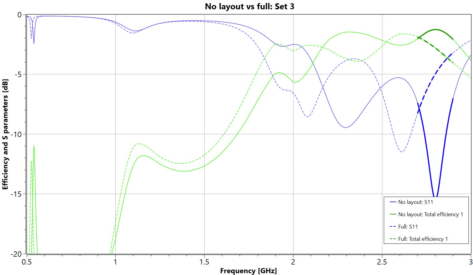
The plots show the comparison between Method 1 (solid lines) vs. the same component values implemented with Method 3 (dashed lines). This comparison brings out the effects of the layout in the synthesis. With the obtained efficiency / S11 results, it is evident that the layout has a major impact: with no layout data, and assuming that the Model 3 represents reality, a realized device based purely on Model 1 data would perform -3.9 dB – (-0.1dB) = -3.8dB worse than predicted. This highlights the value of layout modeling with electrically large elements like switches. As expected, in lower frequencies the effect of layout is not drastic, but at higher frequencies it is!
What is the Effect of Separating Layout from the Antenna?
In this case, we synthesized a matching circuit for 3 bands but using Method 2. Let’s bring the best matching topology from Method 2 as fixed values to the full simulation (Method 3) and compare.
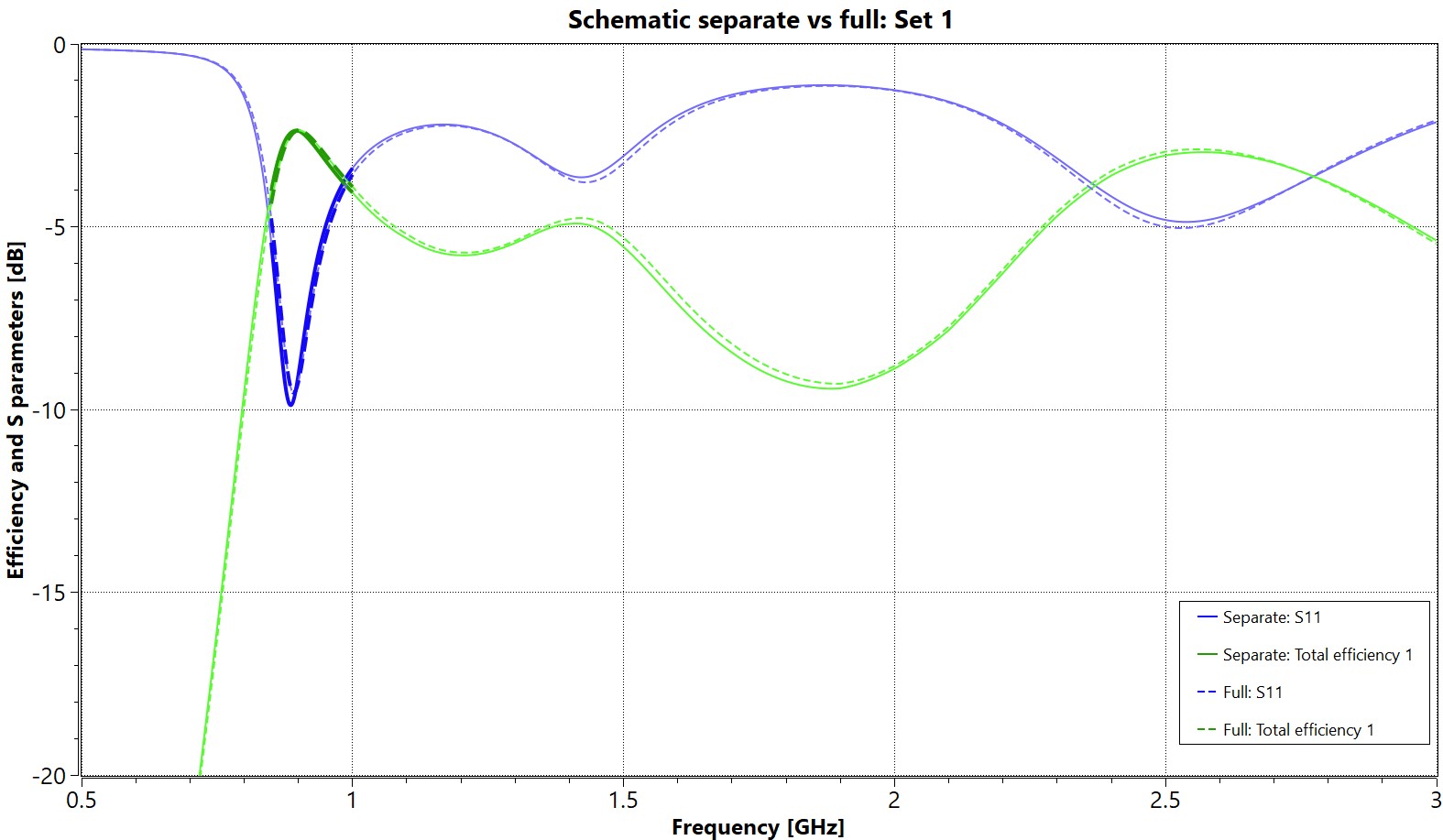
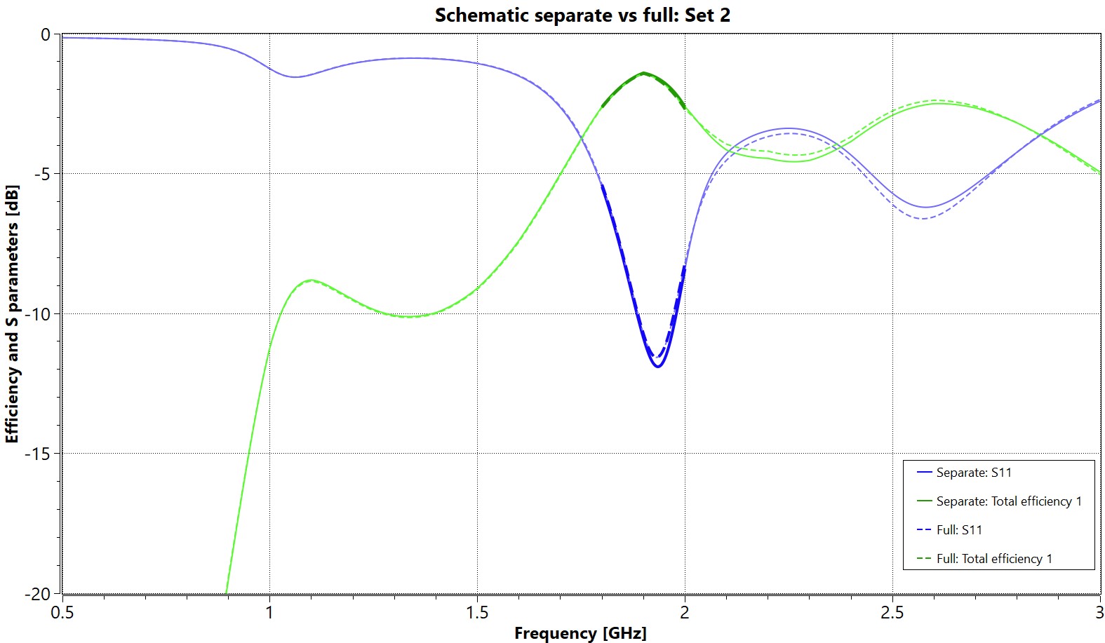
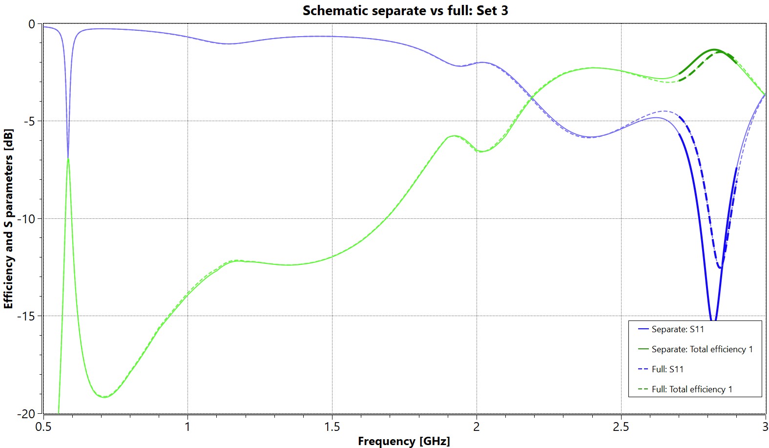
In general, the agreement between Method 2 results (when applied to Model 3) and Model 3 (the full model) is quite good. However, the small shift of the resonance at the highest band indicates that mutual coupling between the layout and antenna physical model may be worth considering. Thus, “to separate or not to separate” the layout from the antenna model needs careful consideration. As usual in engineering, it is ultimately a tradeoff between overall model accuracy and analysis performance.
Summary of the Methods
The teachings of this study can be summarized as follows:
Method 1 (no layout consideration with a simple antenna model):
- Has the fastest synthesis.
- Not well suited for realistic implementation (at least in frequencies above 1 GHz).
- May be used to define an initial matching circuit topology, more accurate methods (2 and/or 3) can continue to optimize the components from this topology.
Method 2 (separate 3D EM simulation of the antenna and the switch layout):
- Works as a compromise between high accuracy and good performance. Two simple 3D EM simulations are usually a lot faster than one big 3D EM simulation.
- The feasibility depends on the EM coupling of the antenna to the layout structure (pads, interconnecting traces) of the switch. With low coupling, this is a very good method.
- The method assumes that the radiation from the switch layout is negligible, and that the layout does not couple electromagnetically to the overall antenna.
- Only the S parameter information of the layout is used which speeds up the synthesis task.
Method 3 (simultaneous EM simulation of the antenna and the switch layout):
- Most challenging in terms of 3D EM computation.
- Takes into account the radiation characteristics of the switch layout and the coupling of the layout to the antenna structure.
Conclusions
Layout effects of switches and tuners may be crucial for accuracy, especially in higher frequencies. The recently introduced Schematic Entry feature of Optenni Lab version 6.0 enables the incorporation of the layout effects accurately and easily with the matching circuit synthesis.
The separation of the EM model into antenna and layout parts speeds up both the 3D EM simulations and the matching circuit synthesis. If the antenna and the layout interact, the accuracy of the method based on such a separation suffers.
As always, modeling is a tradeoff between the desired computation performance and computation accuracy. Optenni Lab version 6.0 offers various ways to easily obtain a good balance between the computation accuracy and time in demanding antenna design and matching tasks.
Field Application Engineer
sergei.kosulnikov (at) optenni.com