In matching circuit design, it is essential to include the effects of the matching circuit layout in the optimization process. Optenni Lab offers multiple ways of considering the layout.
The simplest way is to insert short transmission line segments or microstrip segments between the matching components. These segments can capture the added inductance of the transmission lines and also the ground capacitances of the connecting pads.
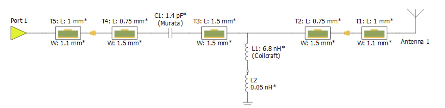
A simple way to take matching circuit layout into account is to use short microstrip segments between the components.
A more accurate way is to use data from electromagnetic simulations for the layout portion of the matching circuit or a switch. Optenni Lab can then optimize the component types and component values using the accurate layout model.
With these tools, Optenni Lab can provide optimized matching circuits which work in real prototypes in a very similar fashion than in simulations. In other words, Optenni Lab can generate matching circuits which work first time right in a real prototype.
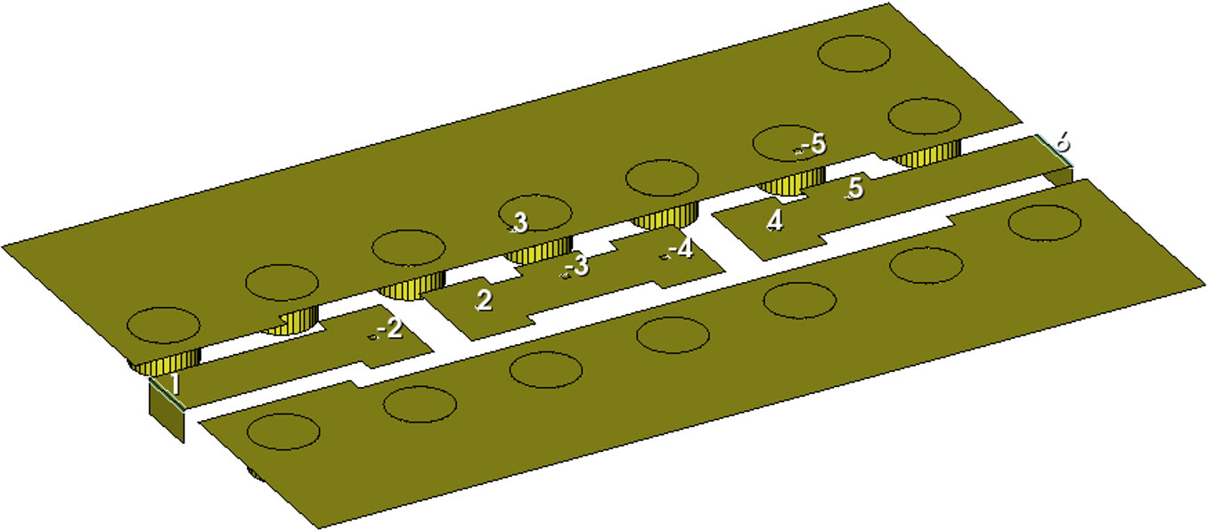
An example of an accurate layout as drawn in an electromagnetic simulator. The simulation data can be easily used in Optenni Lab.
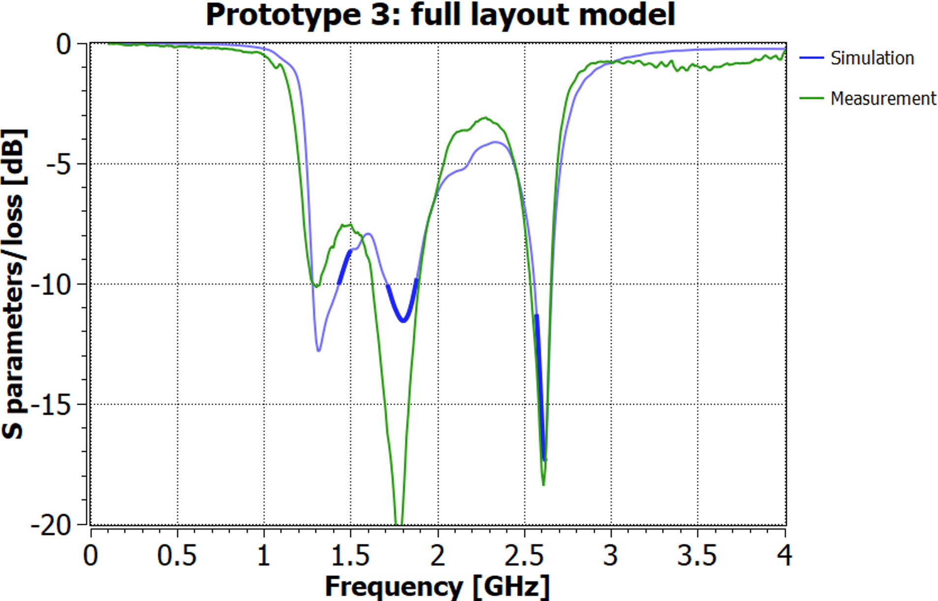
Comparison of the predicted matching circuit response by Optenni Lab (green curve) and the measured response from a protype (blue curve). The agreement is excellent – Optenni Lab can design matching circuits which work in the desired way during the first prototyping round – no further design iterations are needed.
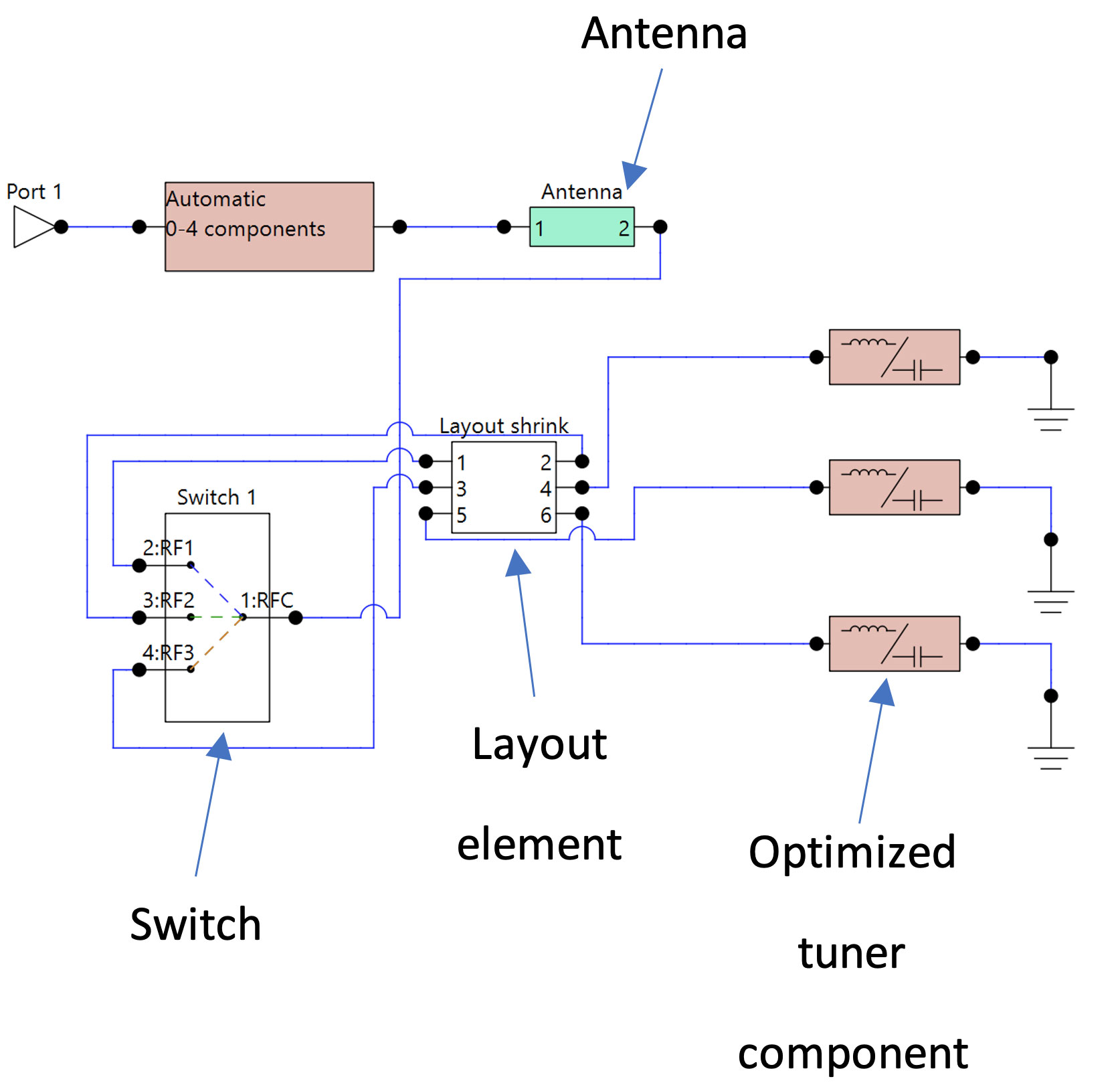
An example of a setup for using realistic EM-simulated switch layout in matching circuit optimization.