The Secret Sauce Behind Tunable Antennas in Wireless Devices

The Secret Sauce Behind Tunable Antennas in Wireless Devices

Posted by Optenni Ltd (originally written by Olli Pekonen) | 26 January 2026

From this article, you will learn about:

  • Complexity of the multi-port multi-antenna design challenge
  • Why the design trend is towards tunable antennas in today’s wireless devices
  • How Optenni Lab speeds up the aperture-tunable multi-antenna design process and performance optimization
  • Tunable antenna design example and comparison to a passive aperture-coupled solution

Introduction

We here in Optenni Ltd take considerable pride in the fact that 7 out of the 10 biggest tech companies trust their demanding antenna optimization tasks to us by using Optenni Lab. But why are we so successful in this market? This article tries to tell the story.

The antenna design challenge in wireless consumer devices

A modern wireless consumer device is a complex maze of various radio technologies, for various communications purposes (cellular, WLAN, Bluetooth, positioning, near field communication, etc.). The devices come in different shapes (e.g. mobile phones, tablets, laptops, smart glasses, smartwatches) — and often must perform reliably in multiple physical states, from hinged laptops to foldable smartphones. Their antennas are suffering from the impedance loading of the person operating them in various ways, and the devices have to operate efficiently to conserve battery power. Additionally, design of antenna radiators is heavily governed by mechanical constraints – long gone are the days of external stub and whip antennas e.g. in mobile phones. This combination of tight mechanical constraints, multiple radio systems, and user-induced detuning makes antenna design one of the most challenging aspects of modern device engineering.

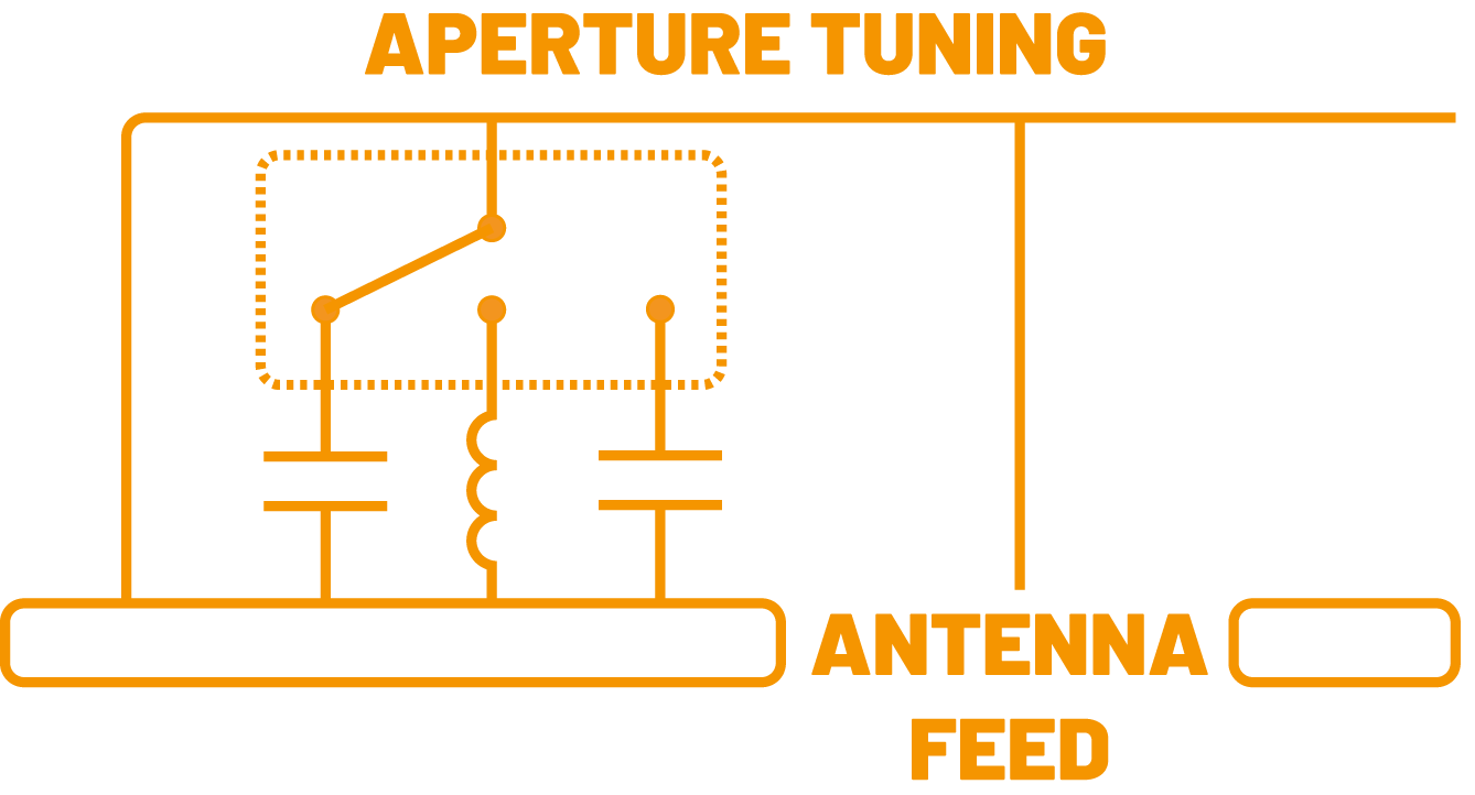
Modern wireless devices comprise multiple antennas, many of which are tunable multi-port antennas using the aperture tuning technology. Aperture tuning enables the same radiator design to operate efficiently across multiple frequency bands.

Of course, the operation of the antenna systems can be simulated with a good quality three-dimensional electromagnetic (3D EM) simulation tool. Just model your device in high-enough detail by placing radiators and their feeding and tuning ports into the 3D EM simulation mimicking reality, and press “simulate”, right?

Well, close, but not quite. To do it right, you still need Optenni Lab!

There are at least four things that are difficult to handle in a contemporary 3D EM tool or RF circuit simulator in the context of a multi-port multi-antenna device.


The design is driven by mechanical aspects and short timespans. Optenni Lab solution: pre-assessment tools that help to weed out antenna radiator designs that will not work, no matter how hard you try to match them.


The matching circuits are complex, but they are produced by the millions. Optenni Lab’s answer: synthesis of the best matching circuit topologies with realistic vendor library components and taking their tolerance variation into account.


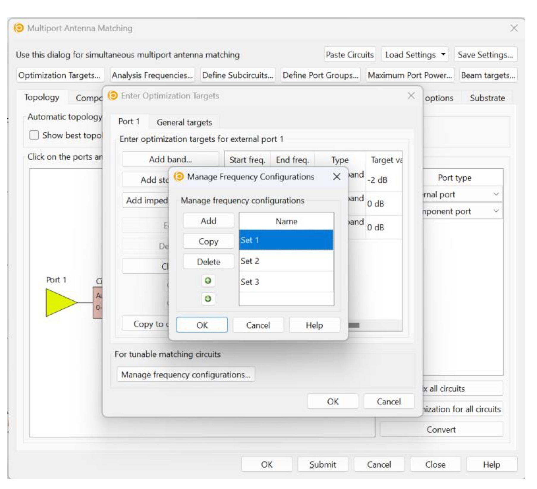
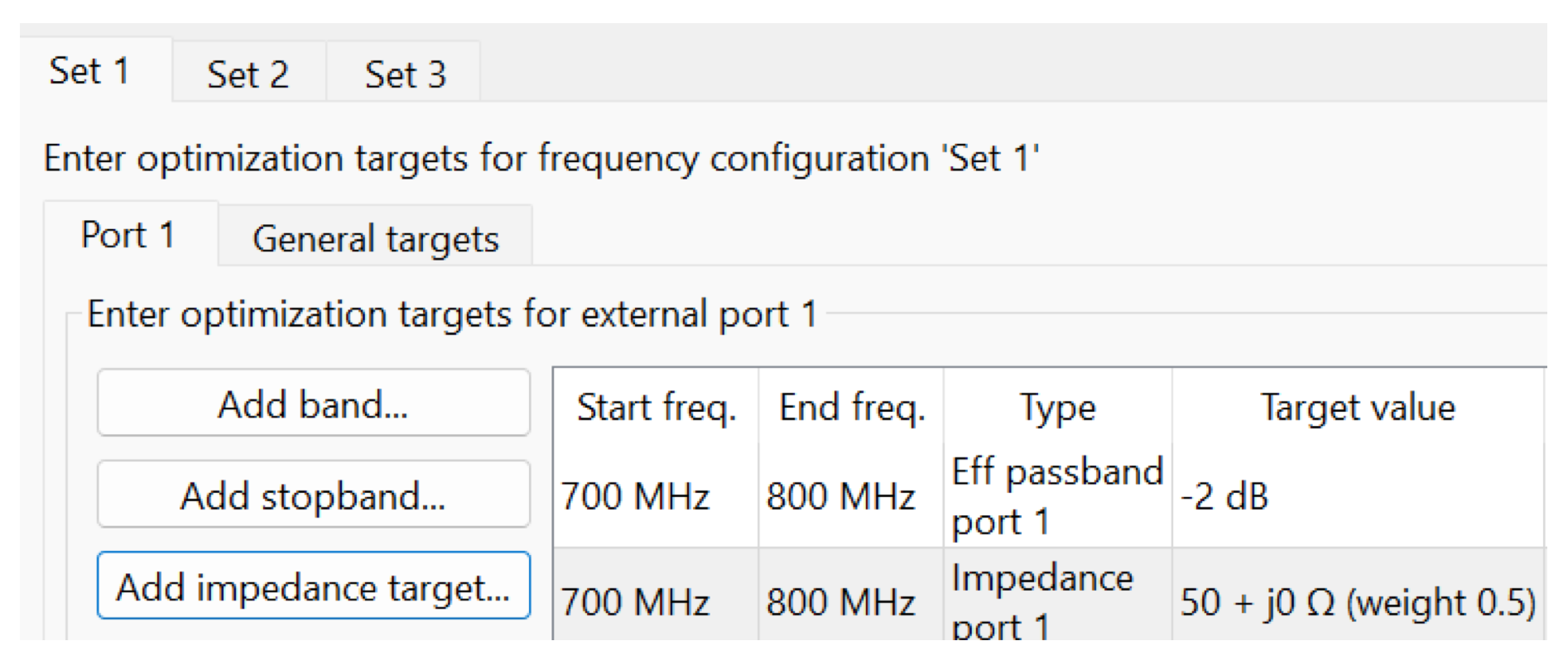
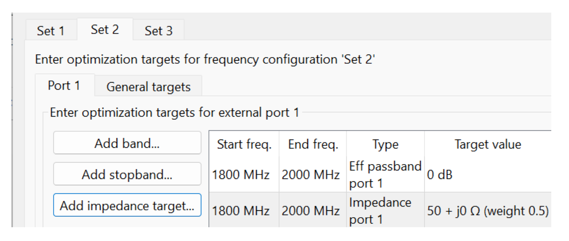
Antenna matching comprises passive and active (e.g. aperture tunable) parts. This is a quite difficult problem as the passive part must be chosen so that it works well with all of the states of the active part. Optenni Lab solution: possibility to honor several frequency responses linked to respective switch/tuner states (a.k.a frequency configurations) for optimal matching.


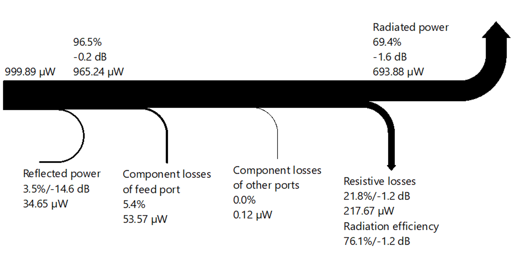
Last but not least: in a wireless product with many antennas and feeding ports, the input power is easily coupled to the other ports, instead of being radiated. In a good design, the matching circuit has a dual role – it must maximize the power transfer to the radiator, and maximize isolation to other radiators. Optenni Lab solution: focus on the total efficiency of the antennas, not just on the reflection at the feeding ports. As the total efficiency is affected by coupling loss, a good efficiency implies low coupling loss. Thus, efficiency focus is a very elegant solution to this problem.


The more complex
the antenna system
is, the greater
benefits you gain
from the Optenni Lab
capabilities during
the design and
optimization phases.

Optenni Lab in Action

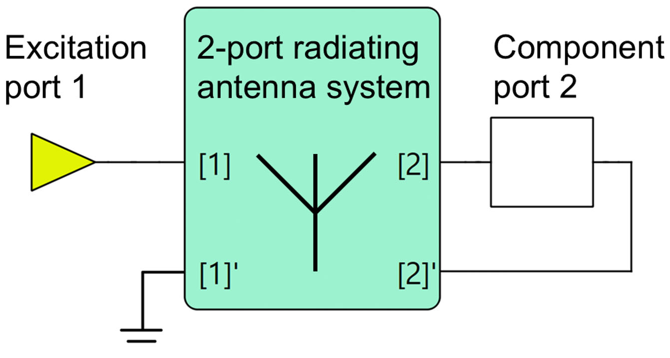
Let’s have a closer look what this means in practice. Consider a simplified handheld device of Figure 1. The device comprises of two aperture tunable antennas, the first, longer antenna 1, positioned at the bottom edge of the device chassis, and the second shorter antenna 2 attached close to the side of the first antenna. First antenna has port 1 as the input port, and port 2 as the aperture tuning port. The second antenna is fed from port 3, and aperture tuned from port 4. Thus, this is a two-antenna system, each antenna comprising two ports: one for input, the other for tuning.

Figure 1: The mobile phone model under study. The ports 1-4 are numbered as follows: Antenna 1: port 1 = input port, port 2 = tuning port, Antenna 2: port 3 = input port, port 4 = tuning port.

For ease of notation, let’s try to design a system where the first antenna operates at example frequency bands B1 (800 – 900 MHz), B2 (1800 – 1900 MHz), and B3 (2800 – 2900 MHz), and the second at B4 (3800 – 3900 MHz), B5 (4800 – 4900 MHz), and B6 (5800 – 5900 MHz), as shown in Figure 2.


This is a demanding
task as it covers,
with just two radiators,
a band ratio of 6:1,
and at considerable
bandwidths (100 MHz each).


Figure 2: Operating bands of the antenna system.

Pre-assessments

Electromagnetic Isolation

Let’s first check out how much unwanted interaction we can expect from the two antennas. The pre-assessment tool for this in Optenni Lab is the Electromagnetic Isolation, which forecasts a worst-case situation (maximum coupling) of any two ports terminated with the most-coupling matching circuits. To maximize the power transfer from feeding ports (ports 1 and 3 in the system), ports 2 and 4 are best left open (if terminated with 50 Ohms, they would eat up some of the signal power between ports 1 and 3, and the forecast is not a worst-case forecast in terms of power coupling between ports 1 and 3).

The result is shown in Figure 3.  Anything above -10 dB is a cause for concern, and for the most bands of interest, we are hovering above -4 dB, sometimes close to -1 dB. It is obvious that just optimizing S11 (or S33),


we would easily end up
heating the termination
of the other antenna,
and little radiation
would ensue


Figure 3: EM isolation between the two feeding ports (ports 1 and 3)

Figure 3 above also illustrates that we cannot separate the two antennas in terms of their matching designs. Realizing a design based on separated simulations, with no regard of the other antenna, would likely exhibit strong coupling, and suboptimal performance. It should be remembered that with multi-antenna systems, the feeding port matching has to cater for both maximal power transfer to the fed antenna and minimal power transfer to the other antennas.

However, as Optenni Lab focuses on total efficiency, the lack of intrinsic isolation is likely not a problem for Optenni Lab derived designs.

Bandwidth Potential

Another aspect that can drive the designer back to the drawing boards because of a failed antenna radiator is the Bandwidth potential. This figure of merit indicates how easy it is to achieve a certain bandwidth at each of the frequencies of interest. Bandwidth potential is one of the many preassessment tools of Optenni Lab.

The results for port 1 are shown in Figure 4, and those for port 3 in Figure 5. Clearly, even with other ports open (to avoid the overly optimistic interpretation of good matching faked by power consumed in the Z0 of the other ports), we more or less have the required 100 MHz bandwidth potential at each of the six bands, bands below 3 GHz, B1 – B3, for port 1, and bands above 3 GHz, B4 – B6, for port 3 (which is the feeding port of the second radiator).

Figure 4: Bandwidth potential seen from the long radiator input port (port 1)

Figure 5: Bandwidth potential seen from the short radiator input port (port 3)

Radiation Efficiency

Finally, as a third figure of merit, it is good to check the radiation efficiency aspect of the system. This preassessment tool is also readily available from Optenni Lab.

Looking at Figures 6 and 7, it appears that we are not limited by the maximum radiation efficiency which could be due to e.g. lossy antenna conductor or any surrounding medium of the radiators. Of course, in the design we need to reach a good radiation efficiency, which is governed a lot by the reactive component in the aperture tuning port. However, looking at Figures 6 and 7, the theoretical maximum performance is -0.5 dB for the antenna efficiency, as this is the maximal radiation efficiency level.

Figure 6: Radiation efficiency of the long radiator (fed from port 1 of the EM model)

Figure 7: Radiation efficiency of the short radiator (fed from port 3 of the EM model)

OK, there is nothing alarming in the starting point of our design – the radiator is not intrinsically too lossy, and the bandwidth potential does not imply a “mission impossible” in terms of matching. Coupling is very strong, but let’s see how Optenni Lab copes with it with the matching networks it proposes.

Antenna optimization methods

For the actual antenna system optimization, we consider the following two methods: active aperture tuning and all-passive (fixed aperture-coupled) methods.

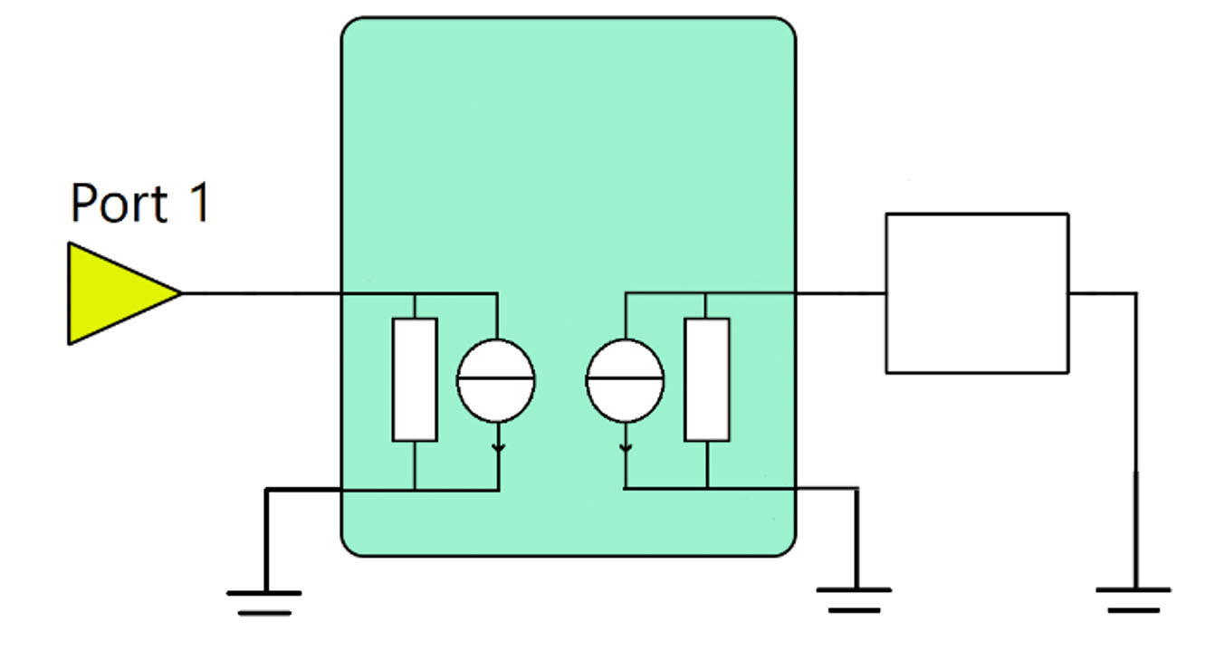
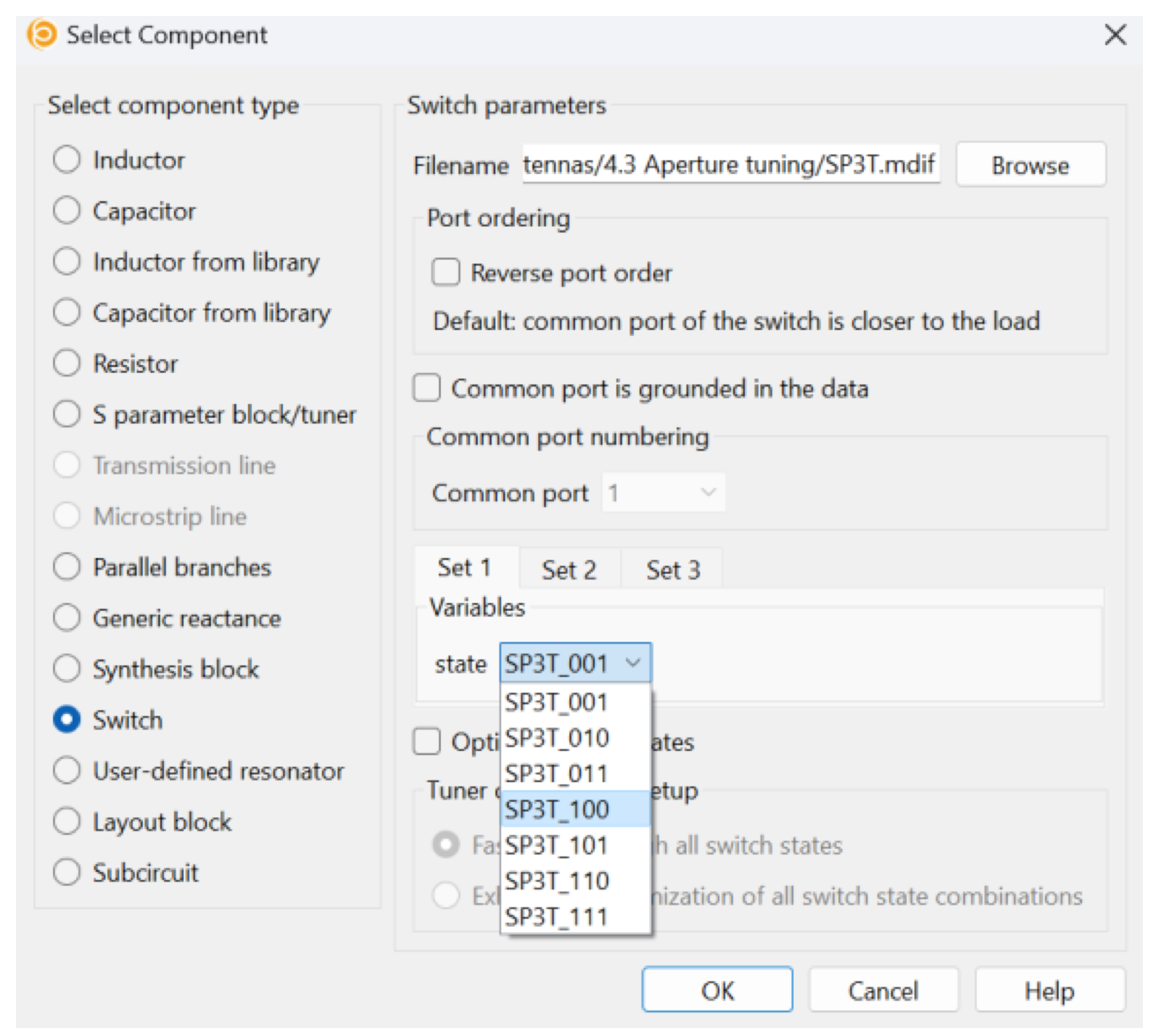
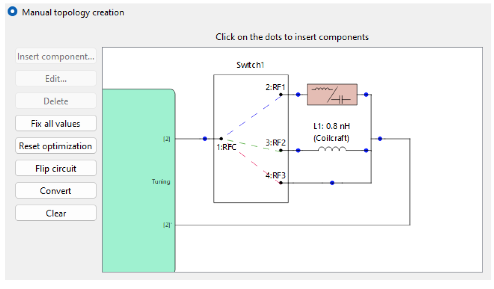
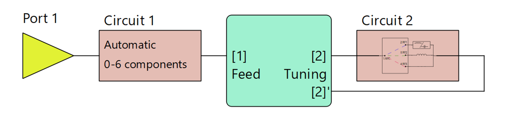
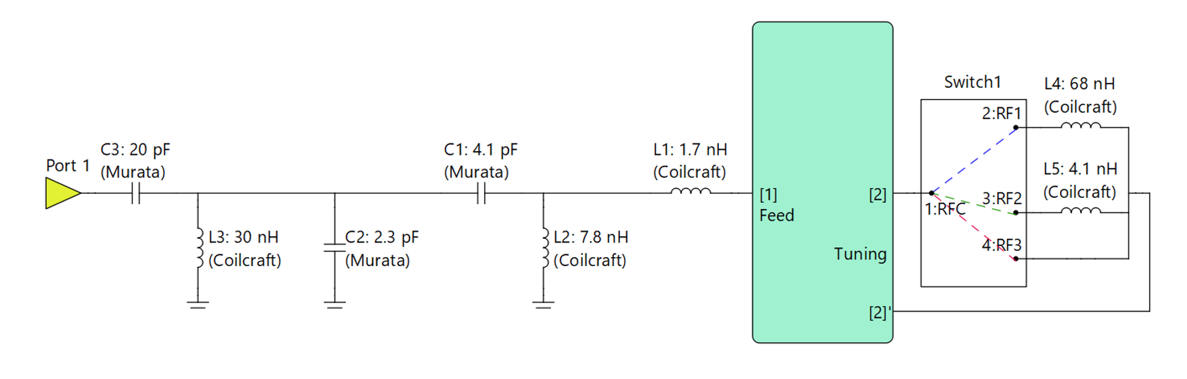
Active aperture tuning method: with two triple-throw switches

The first method is the preferred Optenni Lab way – we use an aperture tuning with a single-pole triple-throw (SP3T) switch at each of the tuning ports. Optenni Lab can optimize the switch states automatically, or the switch states can be pre-defined for the optimization for different operating bands. In both cases, the matching component types and values behind the switches will be optimized by Optenni Lab.

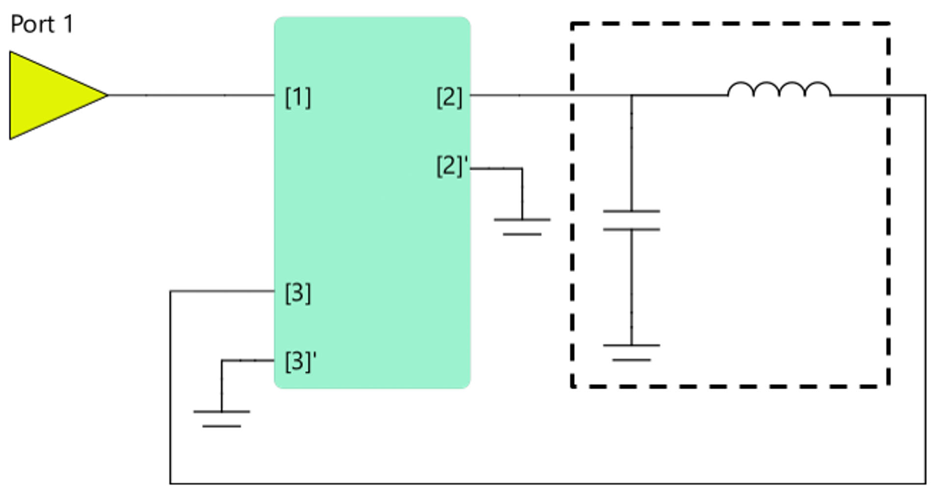
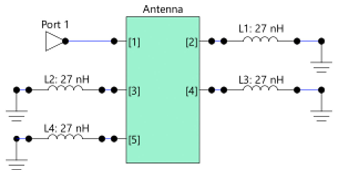
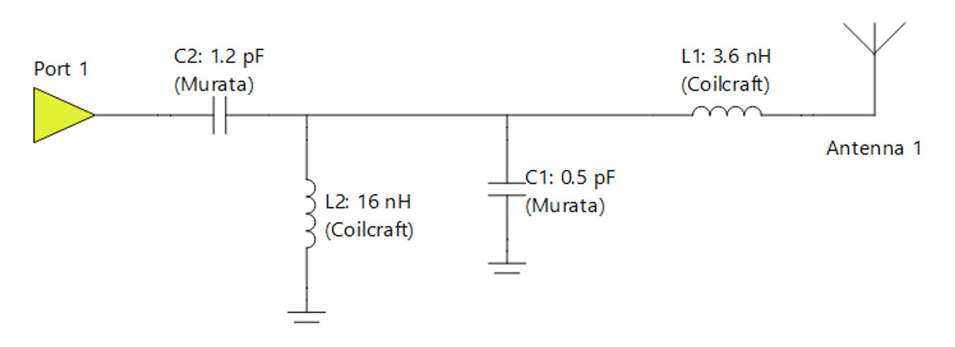
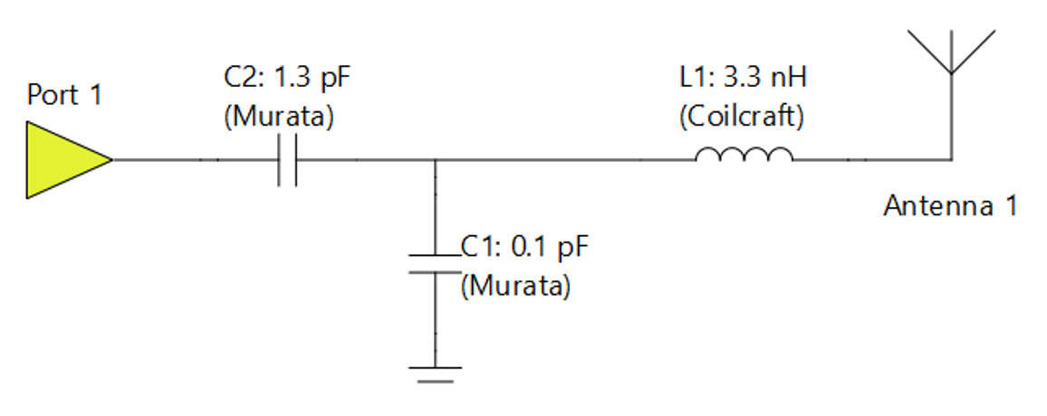
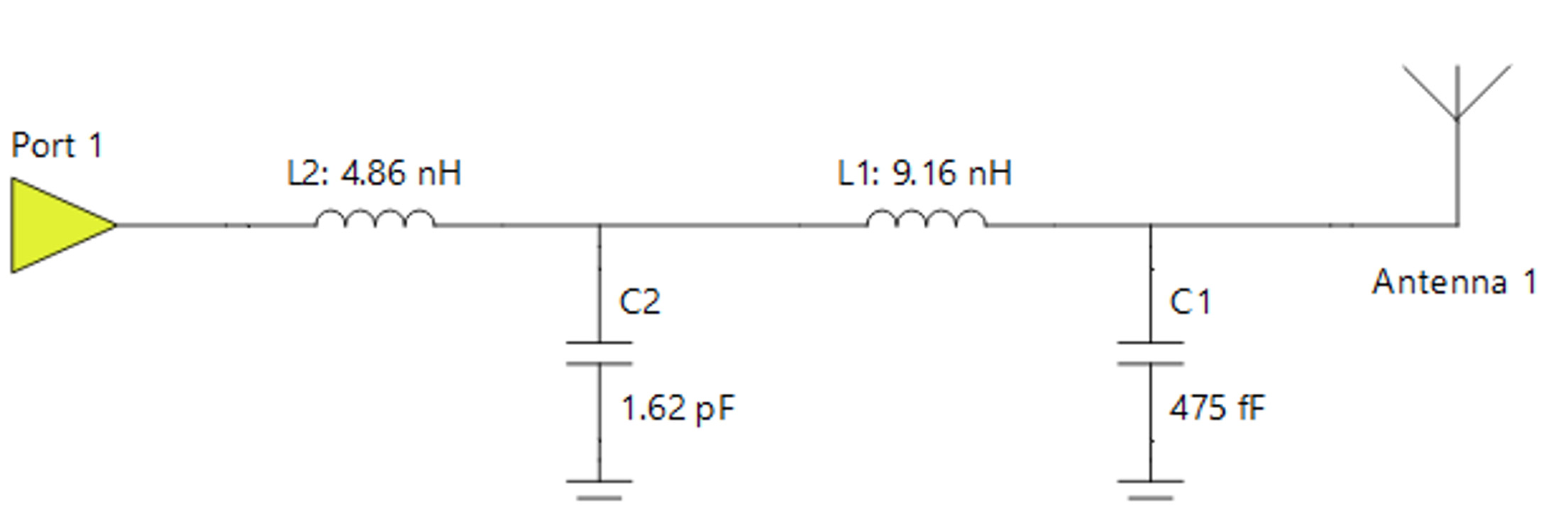
We synthesize a four-component matching circuit into the input ports of the radiators (Circuits 1 and 3), and use the classic multiport antenna matching mode of Optenni Lab. Thus, before the matching circuit synthesis is run, the circuit diagram appears as shown in Figure 8.

Figure 8: Active matching basic topology setup

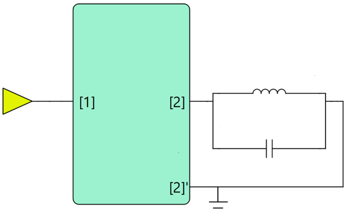
All-passive matching method

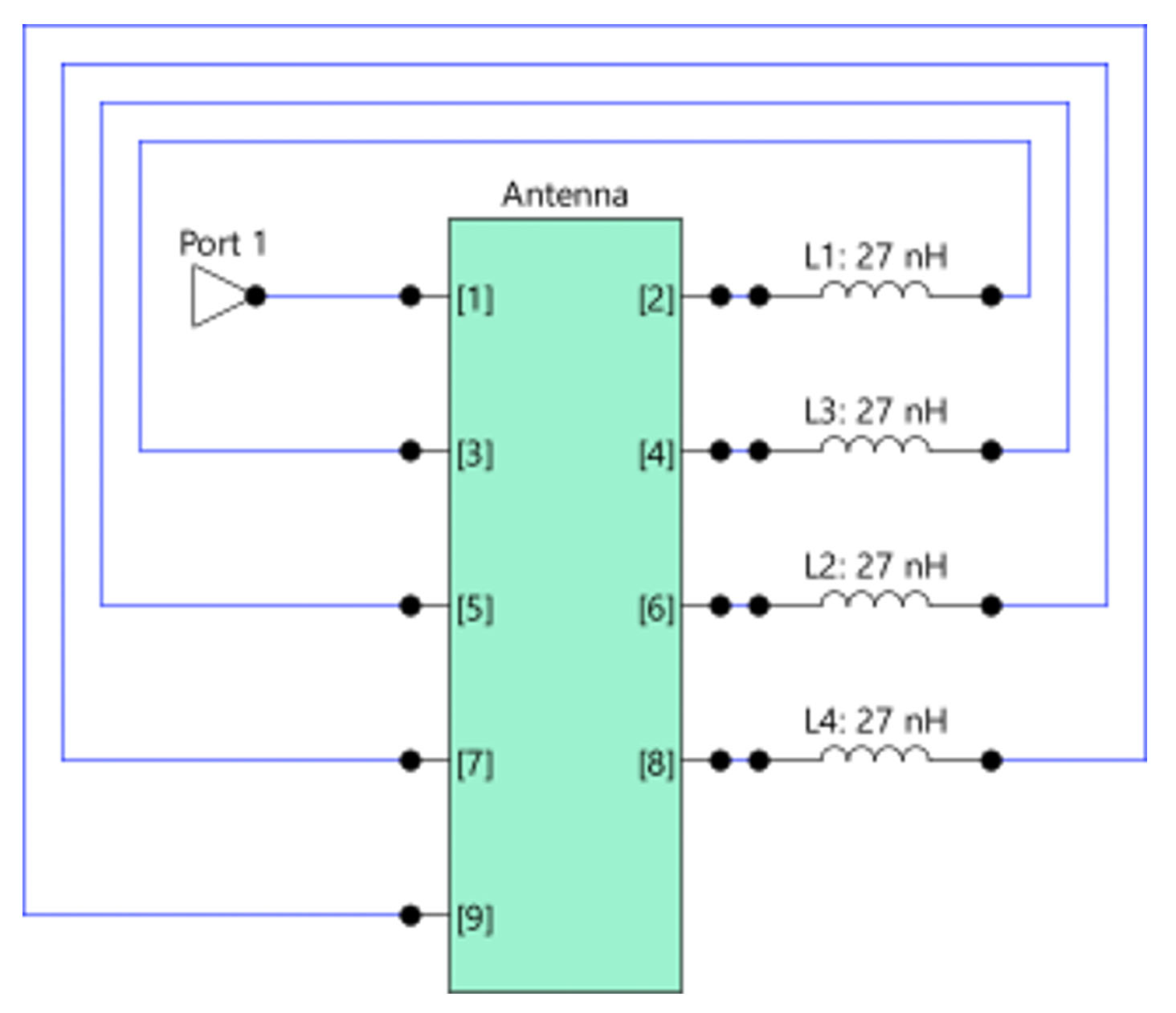
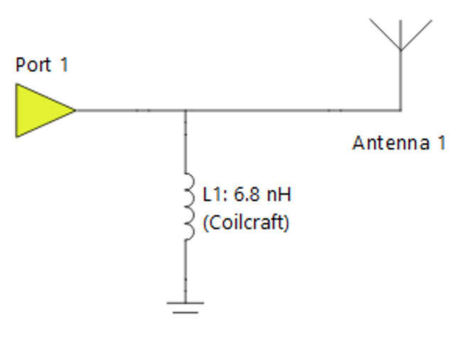
The second option is to use all-passive matching, but having efficiency targets. Here, no switches are used, so the aperture ports are terminated with an element that “best” suits all different bands. This study is very easy to achieve in Optenni Lab. However, note that as the target is related to efficiency, this kind of study is not easy to achieve with circuit simulator tools, even if you would try to guess the matching topology and then optimize the component values (guessing the topology is of course quite tedious and error prone, please use Optenni Lab instead). Before the matching circuit synthesis is run, the circuit diagram appears as shown in Figure 9.

Figure 9. All-passive matching topology

Next, we compare the results band-by-band for the two methods.

Results and band-by-band comparison

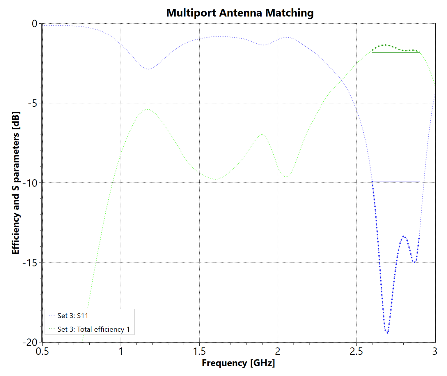
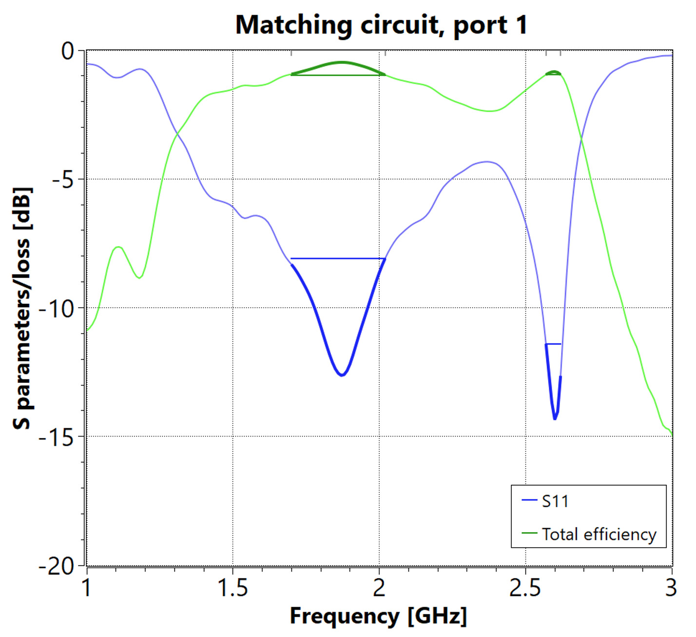
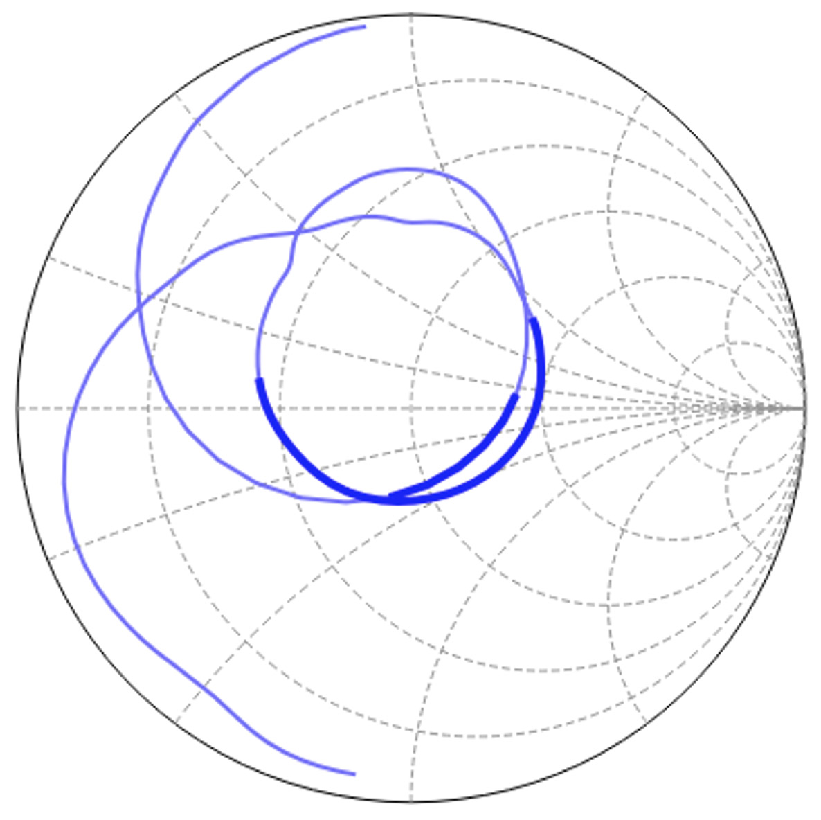
In the graphs below (Figure 10-15), we have the results for both methods and for each of the bands B1 – B6.

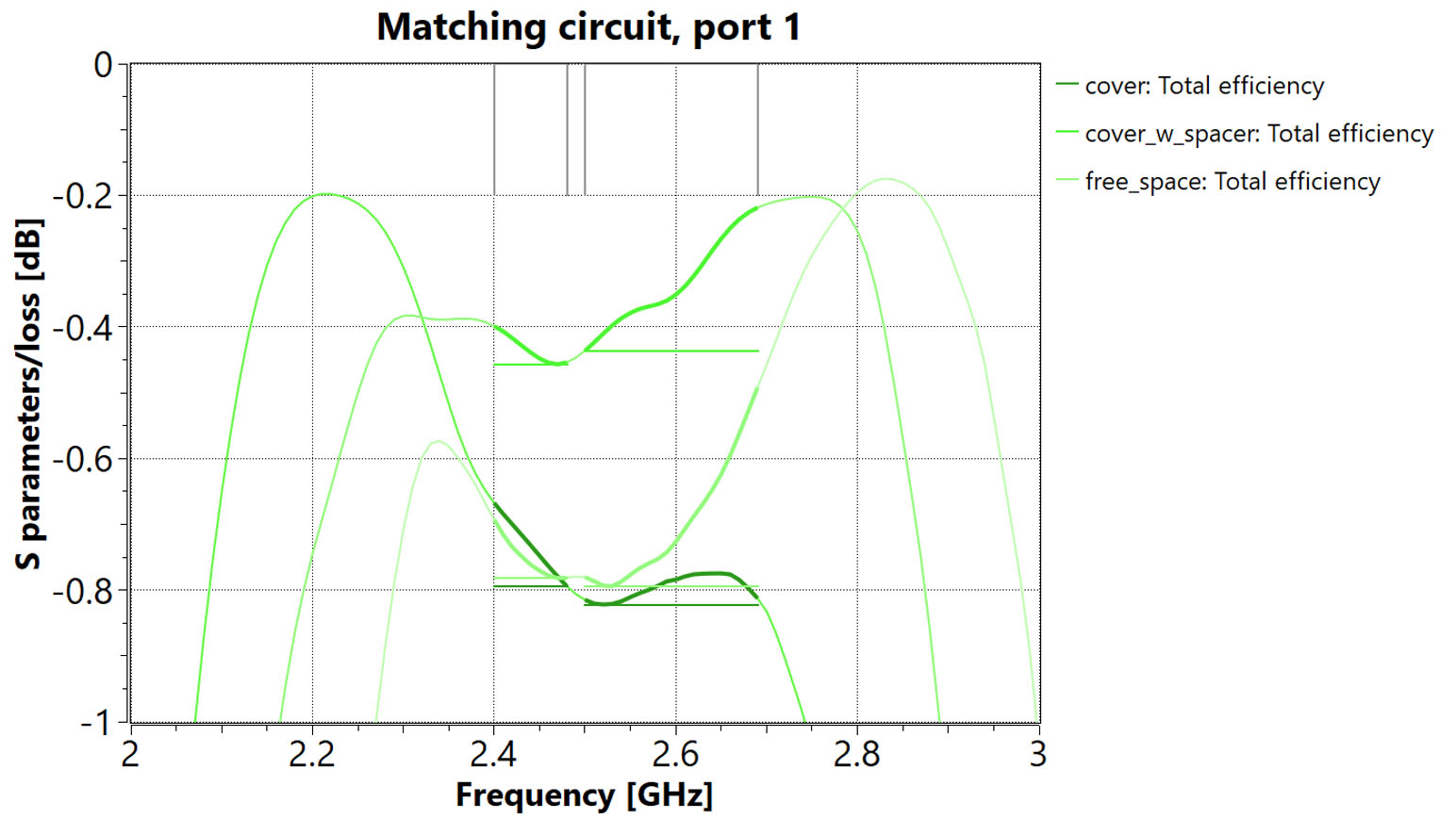
Figure 10: B1 comparison

Figure 11: B2 comparison

Figure 12: B3 comparison

Figure 13: B4 comparison

Figure 14: B5 comparison

Figure 15: B6 comparison

Comparing the results in B1 – B6, it is obvious that the active efficiency-based approach is better, as expected. Actually, the summary of results in Table 1 shows the average values of the total efficiency are even for the two methods on the low band B1. However, the minimum value for the passive approach is worse at the edges of the band. For all the other bands B2-B6, the tunable antenna design performs significantly better than the all-passive approach, and provides over 4 dB total efficiency benefit on band B3.

Table 1. Total efficiency for the tunable and passive antenna design on different operating bands.

Looking into the results B1 – B6 statistically, the average of total efficiency performances over the six bands B1-B6 is as follows:

  • Active, tunable design: -3.2 dB
  • All-passive, non-tunable design: -5.1 dB

This demonstrates the value of active aperture tuning in multi-band, multi-antenna applications.

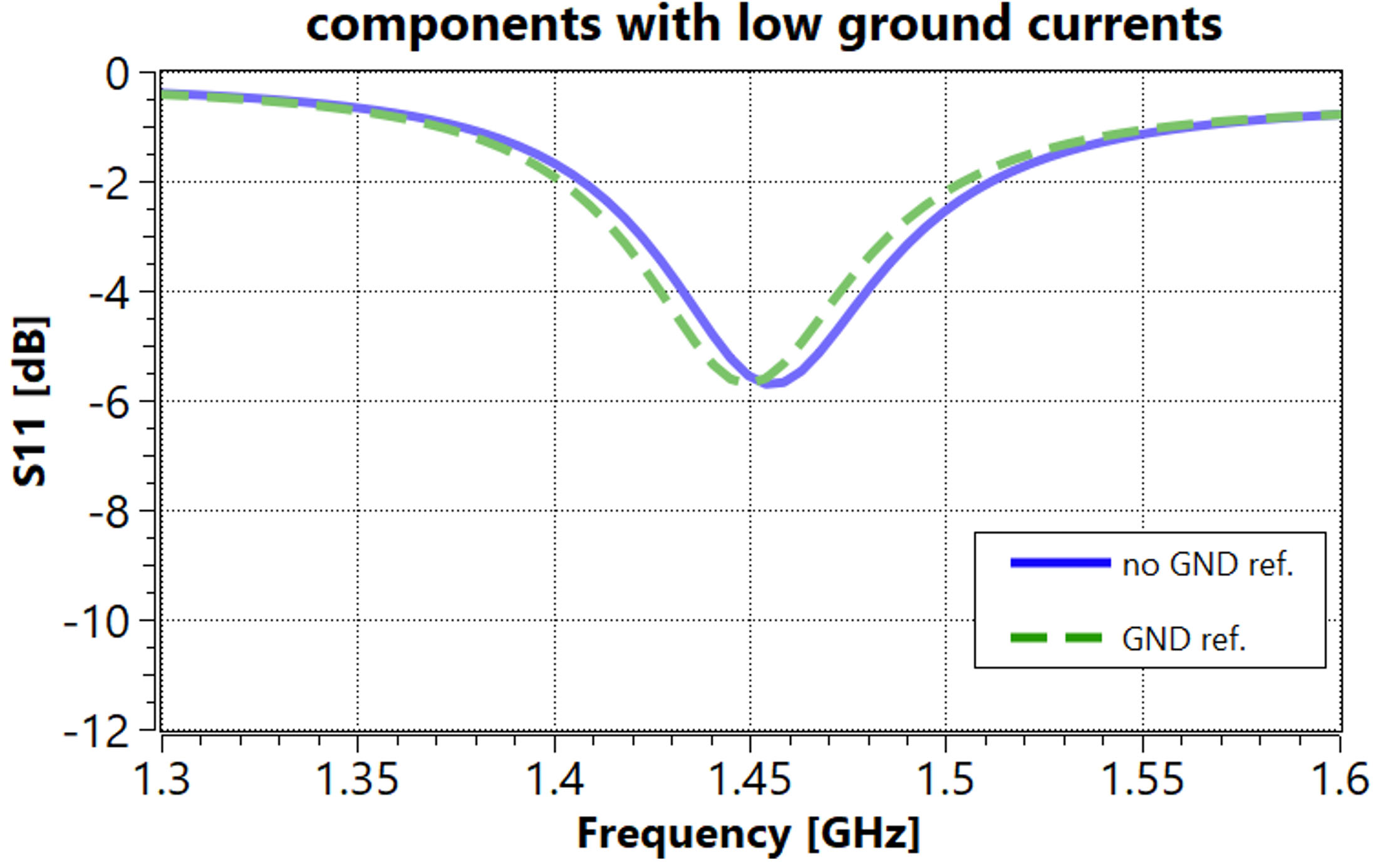
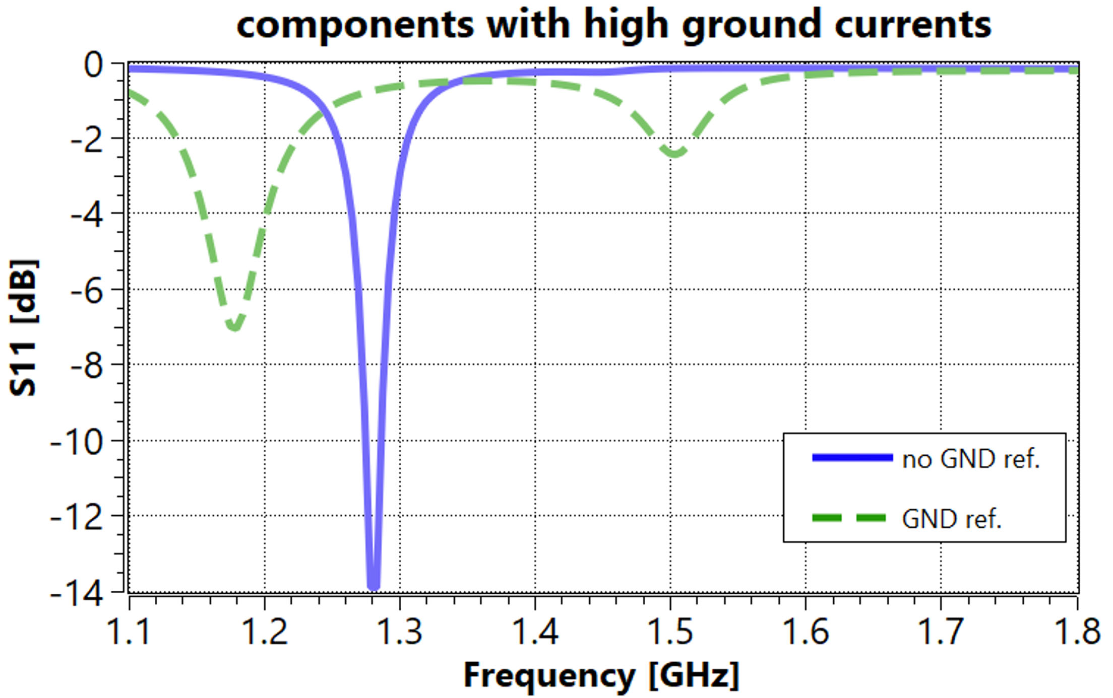
In the pre-assessment step, we analyzed the Electromagnetic isolation between the antenna feed ports. The assessment showed high coupling between the antenna input ports without matching. Based on the total efficiency figures, it’s clear the aperture tunable antenna approach performs better than the all-passive design. However, let’s take a look at the isolation when the matching circuits for all-passive design have been optimized for total efficiency. From Figure 16 we see the isolation between the feeding ports improves significantly after optimization of the matching circuits. The total efficiency performance was automatically synthesized and optimized by Optenni Lab based on the defined optimization targets.

Figure 16. Isolation without matching (same as Figure 3) and with passive matching.

It is worth noting that, although the active aperture tunable design leads to increased component losses due to the additional aperture port elements, each operating state spans a significantly smaller bandwidth. Consequently, a higher radiation efficiency can be achieved in comparison with an all‑passive solution covering multiple frequency bands. The increase in component losses is therefore compensated by the improved radiation efficiency, and the coupling losses between the antennas can be also concluded to be even smaller in the active aperture tunable design than in all-passive based on the higher total efficiency on all the B1 – B6 bands.

Conclusions

In this article, we discussed the factors that make antenna design for wireless consumer devices challenging and explained how aperture tunable antennas can be designed to fulfill today’s product requirements while achieving optimal performance.

We demonstrated the main design steps of a multi-port, multi-antenna system in the context of a simplified handheld device. Based on the results, it is easy to conclude that aperture tunable antenna designs offer clear benefits over an all‑passive approach when an antenna system must cover multiple operating bands within a small mechanical form factor.

Through the design example, we also showcased how Optenni Lab accelerates the design work by providing efficient pre-assessment tools and unique design automation capabilities for matching-circuit synthesis and optimization. Optenni Lab is able to optimally match even the most complex antenna systems found in modern portable devices, whereas multi-port systems are very challenging to co-optimize with other tools available on the market. The more complex the antenna system, the greater the benefits achieved by using Optenni Lab during the design and optimization phases.

While the core Optenni Lab features (e.g., vendor component libraries, tolerance analysis, multi-port matching, and multiple data configurations) are highly relevant for tunable antenna designs, many Optenni Lab capabilities (e.g., frequency configurations and maximum radiation efficiency assessment) have been specifically developed to address complex tunable antenna design challenges. The vendor component library includes RF components for tunable antenna designs, and users can also model custom components using the free MDIF file creator utility available at https://www.optenni.com/technical-resources/. Last but not least, it is worth mentioning that Optenni Lab can be easily integrated into your overall design workflow via supported EM simulator and antenna measurement equipment interfaces.

Do not waste your valuable time by guessing and going through long design iterations. Instead, explore the tunable antenna design capabilities by registering for the Optenni Lab free trial and start using Optenni Lab!

Optenni Ltd
info (at) optenni.com

Unveiling the Impact of Ground Currents on Antenna Matching Circuit Optimization

Unveiling the Impact of Ground Currents on Antenna Matching Circuit Optimization

Posted by Sergei Kosulnikov | 21 November 2025

From this article, you will learn about:

  • Component modeling: the importance of accurate component models
  • How to assess the ground currents and a practical way to evaluate their level for the chosen component candidates
  • Design example showcasing:
    • a recommended approach for PCB layout modeling
    • the impact of ground currents and model accuracy on simulation results

Introduction

In the dynamic world of wireless communication, optimizing antenna performance is paramount. Whether it’s for your Wi-Fi router at home or a satellite communication system in space, antenna matching circuits play a crucial role in ensuring efficient signal transmission. However, achieving optimal performance requires a deep understanding of the intricate interplay between component models and layout considerations, particularly when it comes to the often-overlooked factor of ground currents. In this article, we will show how components exhibiting high ground currents can introduce inaccuracies in the modeling of matching circuits if these ground currents are not accounted for in the simulation.

The World of Component Models:

At first glance, the components used in antenna matching circuits may seem straightforward – inductors and capacitors with just two pins. But beneath this simplicity lies a world of complexity. Internally, these components are represented by two-port networks, and therein lies the challenge. Some component models come with hidden ground currents, which can introduce inaccuracies in our simulations. So, how do we identify these elusive ground currents?

Let’s turn the 2-ports component’s impedance representation into an ABCD matrix:

In a real component measurement, any of ABCD terms can represent a complex number. On the other hand, in the case of ideal series connection of a component with no ground reference, the matrix is represented as:

As shown in [1], the parameter  is a reliable figure of merit for evaluating coupling to ground. This metric provides valuable insight into how coupling may affect simulation results. For components with low ground currents, the resulting value is negligibly small, whereas for component series with high ground currents, the figure of merit approaches or even significantly exceeds unity.

We used this figure of merit for the components in the Optenni Lab Component Library. Our conclusions from the analysis are the following:

  • The majority of manufacturers favour simulation-based models (no ground coupling)
  • Some series are measurement-based only for large values
  • Some series are fully measurement-based
  • Some measurement-based models exhibit problems due to incorrect calibration and de-embedding (non-passivity, unsymmetric behavior or large frequency ripple)

How can I check the component I intend to use exhibits high ground currents?

There is no need for complex analysis, such as transforming the component’s S-parameters into an ABCD representation. Instead, you can build a very simple circuit of the component you intend to use and analyse the resulting Smith chart. For example, let’s pick an inductor, place an excitation port on one side, and leave the other side open:

We selected here two simulation results (they are from the analysis we made to study and demonstrate the figure of merit above). One of the results is for an inductor with low reference to ground currents, and the other one is for an inductor with high coupling to ground currents:

Figure 1. Impedance of two open circuit inductors: (red curve) inductor with low ground currents, (blue curve) inductor with high ground currents.

It is clearly seen from the Smith chart that, in the case of an inductor with low ground currents, all the impedance values are grouped as expected for an ideal open-circuit component (red curve in Figure 1). In contrast, when there is a high level of ground coupling, the curves wrap around the Smith chart, similar to a transmission-line behavior (blue curve in Figure 1). This clearly indicates that the elements cannot be considered ideal lumped components but exhibit a noticeable level of coupling to ground currents.

The Ground Connection Conundrum:

To understand why ground currents matter, let’s delve into the connection between layout and circuit models. Using a two-port S parameter block, we can represent an arbitrary antenna system combined with a component model (Figure 2).  Port 1 corresponds to the antenna feed, while Port 2 serves as a component port for a matching component. This representation allows simulation of any single-port antenna system, for example, an aperture-tunable antenna, and is also valid when the component port is connected in series or in parallel with the feeding port:

Figure 2. Two-port S parameter block with a matching component model.

In fact, the second port of any component in the circuit analysis requires grounding. In case if physical ground connection is lacking, in the circuit analysis the second node is still grounded artificially, so that the equivalent circuit may be represented as follows:

Figure 3. Equivalent circuit for the model with grounding.

Sounds simple, right? Not quite. If there are ground currents lurking within our components, our circuit equations may not tell the whole story. Namely, let’s apply matching, where we explicitly add a circuit with strong coupling to the ground. We will use an inductor as our main matching component, and we can imitate the condition of strong coupling to the ground by adding a component (capacitor) in parallel:

Figure 4. Circuit model with an inductor as the matching component.

However, since we are using the equivalent circuit model shown in Figure 3, adding a ground connection at node [2’] now results in an incorrect parallel resonator (see Figure 5).

Figure 5. Circuit model with a ground connection at node [2]’ resulting as a false parallel resonator.

How can we avoid this effect? Put the main matching component between the nodes of two ports! In this case your topology cannot overturn into the parallel resonator.

Figure 6. Circuit model with a correctly connected matching component between ports [2] and [3].

Navigating Layout Modeling:

Now, let’s talk about a practical example. Picture your antenna’s layout – a meticulously designed circuit board with matching components strategically placed. We use here a simple prototype of PIFA model with pre-defined matching layout:

Figure 7. Simulation model including the PIFA antenna and PCB layout for the matching circuit.

When it comes to simulating this layout, we have several options. The first, simpler method applies a single port for each component without explicit reference to the RF ground:

Figure 8. Layout model with no RF ground connection.

Another approach involves using electromagnetic (EM) simulation, where ports refer explicitly to the RF ground. I.e. we have now two ports, and the second node of each port is connected to the bottom ground:

Figure 9. Layout model with ports referring explicitly to the RF ground.

This way we can set the matching component between the nodes of two different component ports and do reference to ground coupling current. So, here’s the kicker:


ignoring ground currents
in our components can
lead us down a perilous
path of inaccurate
simulations.

Numerical Experiments:

To illustrate the importance of considering ground currents, let’s dive into some numerical experiments applying matching components. We’ll compare two modeling methods: one that ignores ground currents and another one that acknowledges them. In the first case, the component is inserted in the component port. In case if the circuit representation does not show the second node of the antenna circuit block, this second component node should be grounded:

Figure 10. Matching circuit model ignoring the component ground currents (5-port model).

For the second approach we have to connect every component between the corresponding nodes of two ports.

Figure 11. Matching circuit model including the component ground currents (9-port model).

Brace yourself for some surprising results! Let’s see what happens in the case of components with low ground currents applied.

Figure 12. S11 at port 1 using a 5-port model (no GND reference), and a 9-port model (with GND reference), for the circuit with matching components with low ground currents.

The resulting picture is quite good – both methods (using component ports without ground reference and placing the component between two ground referenced ports) match using components with low coupling to the ground currents.

But let’s now check what happens if we use components with high coupling to the ground currents.

Figure 13. S11 at port 1 using a 5-port model (no GND reference), and a 9-port model (with GND reference), for the circuit with matching components with high ground currents.

There is a dramatic difference in results between methods with and without a ground reference for components with high ground currents.

Thus, the conclusion is more than clear.


When ground currents
are neglected, our
matching results go
haywire, especially
with components prone
to high ground
currents.

Conclusions

In conclusion, the impact of ground currents on antenna matching circuit optimization cannot be overstated. While simpler modeling approaches may seem appealing, they can lead us astray if not handled with caution. Here we discuss the pros and cons of two-port approach compared to the more popular single-port approach for lumped-element matching. However, this method requires duplicating the number of component ports used for matching, which can be computationally costly in terms of modelling time. A simpler EM model that uses only one port per matching component and does not reference the RF ground is attractive for simpler simulations of the targeted antenna designs. However, its use in circuit simulation treats the possible ground currents incorrectly. So, next time you’re fine-tuning your antenna matching circuit, remember to keep an eye on those sneaky ground currents – they might just be the key to unlocking optimal performance.

References

[1] S. Kosulnikov, M. Honkala, J. Rahola: ”The Role of Ground Currents in the Co-Simulation of Matching Components and Layout Models in Matching Circuit Optimization”, 18th European Conference on Antennas and Propagation (EuCAP 2024).

Sergei Kosulnikov
Field Application Engineer
sergei.kosulnikov (at) optenni.com

Assessment of Bandwidth Potential with Optenni Lab

Assessment of Bandwidth Potential with Optenni Lab

Posted by Nisatuz Jahra | 3 July 2025

From this article, you will learn about:

  • Antenna assessment method: bandwidth potential and why to use it?
  • How bandwidth potential is calculated
  • How to use bandwidth potential in practice

Introduction

Antennas are characterized by many parameters, of which bandwidth is of especial importance. All communication standards must operate within their allocated frequency bands, which must be well catered by the antenna. An important figure of merit in this study is the so-called bandwidth potential.


An important figure
of merit in this
study is the
so-called bandwidth
potential.

The bandwidth potential of an antenna describes how well it could perform across a range of frequencies if matched using an ideal, two-component lossless matching network. As explained in [1], this assessment is highly valuable for antenna designers, as it helps determine whether a mechanical design is worth taking forward for prototyping and physical implementation, especially when targeting specific applications or wireless standards.

This blog explores how bandwidth potential is calculated using Optenni Lab, and how the tool assists in identifying optimal operating bands for antenna designs. For a broader view of how the concept of bandwidth potential contributes to antenna analysis workflows in Optenni Lab, we recommend reading our earlier blog post, Exploring Antennas with Optenni Lab.

Understanding the Bandwidth Potential Graph

Let’s begin by directly studying an Optenni Lab output graph of the bandwidth potential calculation. The example graph below (in Figure 1) shows the bandwidth potential of an example antenna at Port 1, using a 6 dB reference matching level (the level of return loss the antenna must achieve), across a frequency range from 0 to 6 GHz.

Figure 1: Optimized symmetric bandwidth of a single-port antenna.

Let’s interpret the key features. This antenna clearly has:

  • Strong performance near 2 GHz: The bandwidth potential peaks at around 1200 MHz, indicating the antenna is easily matched with a wide bandwidth in this region.
  • Dip around 3 GHz: A noticeable drop shows that the antenna is more difficult to match with a wide bandwidth here, with bandwidth potential falling below 290 MHz.
  • Second peak near 4.5 GHz: Another region of high bandwidth potential (~900 MHz), immediately suggesting the antenna is suitable for dual-band operation.
  • Lower edge behavior: As usual, the antenna is electrically small at lower frequencies (higher wavelengths) where we can expect it to have very narrow bandwidth characteristics, eventually reaching zero.
    Upper edge behavior: The bandwidth potential falls linearly to zero near the lower and upper ends of the frequency range, which is due to the absence of impedance data beyond the upper boundaries.

What it means for designers

This type of analysis helps designers quickly understand which frequency ranges are naturally supported by the antenna and where additional matching or redesign may be necessary.

How Optenni Lab calculates the bandwidth potential

From a theoretical perspective, bandwidth potential is calculated using RF matching theory within a given frequency range. The antenna is treated as a complex, frequency-dependent load:

Zant(f)=R(f) + jX(f)

Based on circuit theory, any such load Zant(f) can be perfectly matched to a reference impedance (usually 50 Ω) with only two matching components (inductor or capacitor), either in series or in shunt. But this theory holds only for a single frequency, which is of course the narrowest frequency band imaginable.

To calculate the bandwidth potential, at each frequency point, Optenni Lab automatically synthesizes an ideal two-component lossless matching circuit to conjugately match the antenna to a system impedance (usually 50 Ω). It then computes the symmetric bandwidth, i.e. the frequency range symmetrically around the calculation frequency where the return loss stays better than the chosen reference level (e.g., 6 dB in the example). This process is repeated for all frequencies, resulting in a graph that shows bandwidth potential across the frequency spectrum.

In other words, if the original S- parameter or impedance data has 1000 frequency points, the calculation of the bandwidth potential is equivalent to calculating the conjugate matching task 1000 times and recording the obtained symmetric bandwidth for each obtained matching circuit. Note that, for each frequency the obtained matching circuit is different.

In addition to the standard conjugate matching approach, Optenni Lab also offers the calculation of Optimized Bandwidth Potential. As explained in [2], in this method, the software determines the optimal two-component match at each frequency point that yields the maximum obtainable symmetric bandwidth around the center frequency, while still respecting the specified return loss reference level. This provides a more fundamental estimate of the antenna’s true bandwidth capability, independent of any predefined system impedance.

Although the calculation process of bandwidth potential is complex and involves many steps in theory, Optenni Lab simplifies it to just a few clicks, delivering results within seconds (see Figure 2).

Figure 2: Steps to process the assessment of bandwidth potential in Optenni Lab. On the right plot, both approaches of assessment have been illustrated. Result of Standard conjugate matched in blue, Optimized symmetric bandwidth in green.

Detailed View: Conjugate Match to Termination Impedance and Symmetric Bandwidth

As mentioned above, Optenni Lab offers two kinds of bandwidth potential assessment:

  • Conjugate match to termination impedance
  • Optimize symmetric bandwidth

To explore the process further, let’s consider a single-port antenna and analyze how Optenni Lab calculates the bandwidth potential.

Figure 3: S-Parameter data of a single- port antenna (on the left) and standard conjugate matched bandwidth potential of the antenna at a selected frequency 1.73 GHz. This result is also shown in Figure 2.

Figure 3 shows a marker positioned at 1.73 GHz. Optenni Lab always displays the symmetric available bandwidth around the center frequency as the marker value, which in this case is 415 MHz.

Using a 6 dB reference matching level, let’s examine this automatic bandwidth potential assessment result at 1.73 GHz by running a conjugate matching synthesis (see Figures 3-4). At this point, Optenni Lab generates the best combination of a two-component matching circuit, achieving conjugate match and identifying the matched return loss performance.

Figure 4: Conjugate matching at 1.73 GHz to examine the automated result of Bandwidth Potential Assessment.

The result shows that the antenna achieves:

Figure 5: S11 result at 1.73 GHz after conjugate matching around reference level -6 dB.

From this S11 representation, using a reference level of -6 dB, marker L is located precisely at 1.5223 GHz and marker H at 2.255 GHz. This yields a total available bandwidth of 0.7327 GHz (approximately 733 MHz).

Additionally, Figure 5 illustrates the available symmetric bandwidth, defined as twice the minimum distance from the center frequency to the markers. The center frequency of 1.73 GHz is 207.7 MHz away from marker L and 525 MHz from marker H. Consequently, the symmetric bandwidth is calculated, 2X207.7 MHz is roughly 415 MHz as depicted in the figure.

Why Use Symmetric Bandwidth?

Considering a symmetric bandwidth around the center frequency has some key reasons:

  • It provides a consistent and objective way to measure performance around each center frequency.
  • It reflects real-world usage, since wireless bands (like LTE, Wi-Fi, and 5G) are centered around a specific frequency.
  • It aligns with how RF systems are typically designed, balancing performance above and below a central frequency.This can be considered a worst-case scenario, where only the minimum symmetrical frequency band around the center frequency is assumed to be available, extending equally toward both the lower and upper frequency limits.

In the following picture (figure 6), It is illustrated the difference between the S11 results of conjugate matched and maximized symmetric bandwidth around the center frequency 1.73 GHz.

Figure 6: Conjugate matching at the given frequency 1.73 GHz (left) and maximizing optimized symmetric bandwidth around the given frequency 1.73 GHz (right).

Optenni Lab makes bandwidth potential assessment both accessible and efficient. While the underlying process involves detailed matching theory and circuit synthesis, the software automates these steps and presents clear, actionable results. For antenna designers, this is a powerful tool to evaluate and refine antenna concepts before committing to physical prototypes.


While the underlying
process involves
detailed matching
theory and circuit
synthesis, the software
automates these steps
and presents clear,
actionable results.

What predictive value does Bandwidth Potential have?

We have stated many times above that the Bandwidth Potential computation is based on a two-component conjugate matching, which is, in a sense, a quite simple matching approach. Naturally, Optenni Lab supports matching circuits of virtually any complexity. So why not simply use more than two components for a wider band. Should we not get a 5x wider band by using 5x components (that is, ten matching components versus two), right?

Unfortunately, not right!

This matter has been studied extensively in the academia during the heydays of mobile phone development between years 2000 and 2010. A relevant study in [3] analyzed the impact of using more than two components in the matching circuit on return loss and achievable bandwidth. For bandwidth potential estimation, using a two-component lossless matching network offers a practical balance, ensuring realistic results while maintaining an acceptable return loss level.

To emphasis on the statement mentioned above, let’s check some analysis done in [3],

Figure 7: Percentage of the theoretical maximum impedance bandwidth that can be obtained with a resonant antenna having an ideal lossless matching network as a function of the number of resonators in the system. The first resonator (n = 1) represents a resonant antenna. The matching circuit contains n − 1 resonators. And one resonator consists of two circuit elements (inductor or capacitor).

Figure 7 illustrates the relationship between the number of matching resonators and the percentage of the theoretical maximum achievable bandwidth. As shown, using a two-component matching network already provides approximately 60% of the maximum theoretical bandwidth, offering a practical and efficient balance for bandwidth potential assessment. While additional components can further increase the bandwidth to around 90% of the maximum theoretical bandwidth the improvement saturates quickly. This analysis indicates that a maximum of 1.5x bandwidth enhancement with respect to the bandwidth potential result can be achieved by adding more matching components. In other words, if 200 MHz bandwidth is required, but bandwidth potential shows 100 MHz, the required bandwidth will not be reached by using any number of lossless components.

For bandwidth potential analysis, sticking to two-component matching is sufficient and realistic to predict the best-case achievable bandwidth without overestimating due to overcomplicated matching networks. And by multiplying the bandwidth potential by two, you are very close to the theoretical limit which is virtually never reached with real life lossless circuits.


Why did we
mention the word
“lossless” above?

Well, you can always improve matching with losses (in the extreme, try a 50 Ω resistor as your antenna – what a wonderfully wide band, and what a horrible level of useful radiation). In general, the only way to get a good radiation and total efficiency is to minimize Ohmic losses in the process, even when they make the matching for a wide band harder.

Conclusions

Optenni Lab provides antenna designers with an efficient method to assess bandwidth potential using a two-component, lossless matching approach. This ensures realistic bandwidth estimation without the complexity of multi-component matching circuits. While adding more components can slightly improve bandwidth, Optenni Lab’s approach offers a practical balance between achievable bandwidth and design simplicity, supporting faster, more reliable antenna development.

References

[1] J. Villanen, J. Ollikainen, O. Kivekäs, and P. Vainikainen, “Coupling element based mobile terminal antenna structures,” IEEE Transactions on Antennas and Propagation, vol. 54, no. 7, pp. 2142-2153, 2006.

[2] J. Rahola, “Bandwidth Potential and Electromagnetic Isolation: Tools for Analysing the Impedance Behaviour of Antenna Systems,” presented at the European Conference on Antennas and Propagation (EuCAP), Berlin, Germany, March 23-27, 2009.

[3] J. Ollikainen, Matching Circuit and Antenna Structure Effects on the Bandwidth of Impedance Matching, Doctoral Thesis, Helsinki University of Technology, 2004.

Nisatuz Jahra
Account Manager
nisatuz.jahra (at) optenni.com
Ready for a free Optenni Lab trial?
Contact us for a product demo and further information on the latest Optenni Lab features


Mastering antenna impedance measurements (at 4-10 GHz) – Volume II

Mastering antenna impedance measurements (at 4-10 GHz) – Volume II

Posted by Jaakko Juntunen | 16 June 2025

From this article, you will learn about:

  • Design challenge: sources of error in vector network analyser (VNA) impedance measurements and simulation models affecting the matching circuit synthesis and verification
  • Step-by-step example for the impedance measurement and verification methods recommended for the frequency ranges above 4 GHz

Introduction

Our previous blog article covered impedance measurement calibration for the design problems below 4 GHz. Our conclusions included two recommended methods, Port extension and On-board calibration, that demonstrated strong alignment between measured and simulated results within the frequency range. However, the logical question after mastering the measurements below 4 GHz was:

How about higher frequencies, for example, the measurements needed for UWB or 5 GHz WLAN systems? Controlling the measurement and simulation model accuracy gets harder as new parasitic phenomena enter the scene, requiring a refined approach.

In this article, we focus on impedance measurements within the 4 – 10 GHz frequency range, which encompasses a variety of interesting applications.

Why 8 GHz is harder than 2 GHz?

We can identify several factors that contribute to uncertainties of matching circuit simulation models, thus causing modelling errors and eventually discrepancies between the measurement and simulation. We can readily study the influence of the following:

1) Ideal versus library component models
2) Non-ideal grounding of shunt components
3) Uncertainty of reference plane location
4) Matching circuit component interconnects have non-zero size
5) Signal transition inductance from measurement pigtail onto the signal line

Factor 1): Ideal versus library component models

When we consider typical 0402 or 0201 package size chip capacitors/inductors, Factor 1) becomes a dominating source of error when going from 2 GHz to 5 GHz and higher. As an example, we simulate the S11-response of an antenna with a matching circuit assuming (a) ideal component models and (b) using library component models with the same nominal values as in case (a).

The matching circuit design target is a dual-band response at 5.5 GHz and 7 GHz. The difference between (a) and (b) deviates strongly above 3 GHz. It is interesting to look at the difference |S11,ideal – S11, library| over frequency, Figure 2, where the difference is measured as the distance between the S11 values within Smith chart. A difference of 0.1 can be considered small, and in this example the corresponding upper frequency limit is 3.13 GHz. The difference increases rapidly at higher frequencies, reaching 0.5 (half the radius of Smith chart) at 4.2 GHz. This study is one explanation why the use of vendor library models can be somewhat relaxed below 3 GHz, but must absolutely be used at 5 GHz or above.


Figure 1: Simulated S11-response of a matched antenna using the same matching circuit, but assuming ideal components (blue curve) or using vendor library component models (green curve)


Figure 2: Absolute value of the difference between complex reflection coefficients assuming ideal components or vendor library component models

Factor 2): Non-ideal grounding of shunt components

In a typical scenario the shunt component ground is not exactly equal to the signal ground. The top ground layer is usually nailed by vias to the ground layer below the signal trace, and thus there is an inductive return current path from the negative terminal of the shunt component to the signal ground. As a rule of thumb, one may expect inductive grounding in the range of 0 – 0.2 nH, which may sound small, but let’s look at its impact closer.

Motivated by the findings of Factor 1), we re-design the matching circuit using library component models for a dual-band response at 5.5 GHz and 7 GHz. We then check the impact of additional 0.2 nH inductance to the shunt components, Figure 3. We observe a big impact, Figure 4.

Figure 3: Dual-band matching circuit, with 0.2 nH extra inductance added to the shunt component simulation model


Figure 4: Comparison of matched antenna response assuming ideal versus inductive grounding of shunt components

However, it is not true that assuming 0.2 nH extra shunt inductance always has such a big impact, even if the frequency is high. Therefore, we cannot state a general rule here, but it is easy to check the hypothetical impact, and if it is significant, be prepared to adjust the simulation model as described shortly.

Factor 3): Uncertainty of reference plane location

Even a carefully calibrated measurement involves some uncertainty regarding how well the effective reference plane agrees with the first matching component model’s reference plane. This may cause big enough phase rotation that makes the matched response to deviate far from the target. Figure 5 illustrates the phase rotation due to 1 mm shift of the reference plane, causing 40 degree rotation at 8.5 GHz. If we assume zero shift in the reference plane, but if there is 1 mm shift in reality, the optimized matching circuit works poorly.


Figure 5: Unmatched antenna S11-response with and without assumption of 1 mm shift of the reference plane. Marker at 8.5 GHz.

Factor 4): Matching circuit component interconnects have non-zero size

Optenni Lab offers two methods to model the board layout of the matching circuit: EM-simulated Layout block or a simplified model based on transmission line segments. While Layout block can model arbitrary geometries covering also shunt grounding issue of Factor 2), if the layout is a simple chain, a simplified model often provides sufficient accuracy. Further benefit of the simplified model is that its dimensions can be optimized. Therefore, uncertainties related to component models’ effective reference planes can be absorbed in these dimensions.

The interconnect dimensions have a big effect to the matching circuit operation, as is demonstrated in Figure 6.

Figure 6: Comparison of matched antenna response assuming ideal versus finite connectivity between the matching components

Factor 5): Signal transition inductance from measurement pigtail onto the signal line

When a pigtail is soldered on the board, the signal experiences a discontinuity when it exits the coax shell and propagates down the transmission line towards the antenna. Typically, this discontinuity is equivalent to about 0.5 nH lumped inductance. This inductance is present in the measured impedance but not when the device is operational. Therefore, if the impedance is not corrected for this inductance, we are introducing an error to the matching circuit design input data. Once again, the impact may be significant as illustrated in Figure 7.

Figure 7: The green curve shows the S11 response if there is 0.5 nH signal transition inductance in the measurement of the unmatched antenna, while the blue curve represents the designed response omitting this inductance


To summarize, each
of the Factors 1)-5)
can have a big
impact on the success
of the matching circuit
design, explaining
“why 8 GHz is
harder than 2 GHz”.

In the following chapter we explain how to bring all these factors under control so that we can design a working matching circuit also at high frequencies.

How to bring all these parasitics under control?

There are two keys to success in this matching challenge. The first is the use of accurately calibrated pigtails. Optenni partners with Dicaliant Ltd, who delivers calibration kits and compatible measurement pigtails for frequency categories from 4 GHz up to 8.5 GHz. The second key to success is to follow a sequential measurement-modeling sequence. The method incrementally improves the model accuracy, and the design target is typically achieved on the first attempt or in just one iteration. We will consider this sequence next.

Step 1: Measurement of open-ended short segment of feedline

It is a useful checkpoint to begin by measuring only the matching circuit layout section such that all shunt components are unpopulated and all series components shorted, except the one closest to the antenna, see Figure 8.

Figure 8: Suggested first measurement step

This step serves several purposes: it validates quantitatively the RF grounding of the feed line (does the response look like that of an open-ended transmission line?), it characterizes the substrate (how many degrees phase delay there is for X mm of the line), and it characterizes Factor 5) above, the pigtail landing inductance. In practise, a simple model is fitted to the measured response, which is then very easy to de-embed from the subsequent measurements, see Figure 9.

Figure 9: Example circuit resulting from model fit to measured open-ended transmission line segment

Step 2: Measurement of unmatched antenna

In the second step, the remaining series component gap is also shorted, and thus we are measuring the impedance of the unmatched antenna. The pigtail is not moved, so the parasitic landing inductance is the same. By de-embedding the model of Figure 9 from the result takes the calibration reference to the first matching component closest to the antenna, to be compatible with Optenni Lab synthesis. The de-embedding can be done explicitly in Optenni Lab by adding a negative inductance and negative length transmission line in series with the measured antenna data (note the flipped order of components, subtract inductance first). The de-embedding causes a counterclockwise de-rotation of the S11-trajectory in Smith chart, Figure 10.

Figure 10: Unmatched antenna S11-response before and after de-embedding of the transmission line segment from pigtail tip up to the first matching component

Step 3: Synthesize, implement and measure a matching circuit

Next step is to use Optenni Lab to synthesize a candidate matching circuit. You can already include a coarse interconnect model between the matching components. This partly tackles Factor 4), and use of vendor component libraries in the synthesis tackles the most important Factor 1) in the list of error sources. The synthesis is carried out typically using generic reactance components in Optenni Lab, providing multiple optimized topologies in one go. Figure 11 shows the simulation vs measurement for the resulting first candidate circuit (synthesis carried out with library components for generic reactance components). We observe a noticeable difference between the simulated and measured result.


Figure 11: Simulation vs measurement of the 5.5/7.0 GHz dual-band design (above), first candidate circuit (below)

Step 4: Adjust the simulation model to fit measured response

There are still several nonideality factors that we can cover in a single adjustment step. First, to account for Factor 3), uncertainty in the reference plane location, we add an optimizable transmission line with zero nominal length, and optimization length range including negative and positive values. This allows moving the reference plane towards antenna or away from it. Second, to account for Factor 2), the non-ideal grounding of shunt components, we add inductances of zero nominal value to the shunt components, with optimization limits of 0 – 1 nH. Third, to improve resolution of Factor 4), we optimize the length of the interconnect models between components.

The optimization target for the simulation model is to find parameters which make the simulated S11 agree with the measured S11 over the whole measured frequency range. A successful model fit is indicated by the cost function value of -2.0 or higher, and for example cost = -1.0 is considered an excellent fit. Please note that to compare apples to apples, we must include the pigtail landing inductance in the simulation model. In this example, we reach a good model fit with cost = -1.8.

Step 5: Re-optimize the component values to meet the target

If the layout model fit is good, we have the physical response under control. Fixing the layout model and re-optimizing the component values, often a single iteration is enough to reach the target. In our example, two iterations were needed, mainly because the higher resonance is very sensitive, but the resulting simulation vs measurement agreement is really good, Figure 12.

Figure 12: Simulation vs measurement after re-optimization of the component values. Coarse component value grid in the capacitor library prevents exact tuning of the higher band of the example antenna to 7.0-7.2 GHz.

Conclusions

We have discussed many roadblocks that hinder simulations to agree with measurements, especially when dealing with matching circuit design above 5 GHz. There are two things required for smooth design success: an accurate pigtail calibration kit, and a careful modelling-measurement sequence. The checkpoints in the process provide a possibility to review the prototype or simulation model early. Following these principles often provides a satisfactory result, even on the first attempt or after just one adjustment iteration.

Jaakko Juntunen
Account Manager
jaakko.juntunen (at) optenni.com

Mastering antenna impedance measurements – Volume I

Mastering antenna impedance measurements – Volume I

Posted by Jaakko Juntunen | 8 April 2025

From this article, you will learn about:

  • Design challenge: sources of error in vector network analyser (VNA) impedance measurements affecting the matching circuit synthesis and verification
  • VNA measurement methods recommended for the frequency ranges up to 2-3 GHz
    • Port extension method
    • On-board calibration method
  • Impedance measurement example and verification

Introduction

Your RF and antenna design flow may start from a 3D EM simulation model of an antenna, selecting a suitable catalogue antenna, or directly from an antenna prototype. Whatever is the end-to-end design flow, prototype measurements and verification steps will be eventually needed to match the design with the target specification. Optenni Lab can greatly accelerate your design flow with the matching circuit synthesis, and it can also interface with VNAs in real time. A shortcut to guaranteed success in circuit synthesis and prototype verification is the correctly measured impedance data.

Measuring antenna impedance is hard. You might protest and say: “how come, just take a VNA, connect it to the antenna and there you go!”


The keyword
here is connect
how do you
actually connect
to the antenna?

Perhaps your protest in fact describes measuring a chain of antenna, transmission line and a connector? I agree – this is easy. But it is surprisingly tricky to get around the influence of the connector and the transmission line between the connector and the antenna.

Often there are no connectors anyway. Let’s just think of an SMD antenna module, or antenna formed by shaping the metallization on a PCB. The antenna should be matched such that the RF chip RF node is loaded by a specified impedance, typically 50 Ohms. Both the matching circuit design and the result verification require measurement of the impedance on a specific location on the PCB (see Figure 1).

Figure 1: Sketch of on-board measurement setup. Location A. for antenna impedance measurement, and location B. for antenna + matching circuit impedance measurement.

In Figure 1, the location A. refers to the point where antenna impedance is measured (before matching circuit design) and that measurement gives the input data for Optenni Lab circuit synthesis. Impedance measured at location B. refers to the point where the impedance of antenna and matching circuit combination is measured, and that measurement gives the input data for the design verification. Measuring the impedance correctly at these two points is critical for the matching circuit design and verification, as the errors in antenna impedance measurement means that incorrect input data is used in matching circuit synthesis leading to potentially huge errors in realized impedance, and errors in design verification impedance data hampers making correct conclusions about the success of the matching.

In this article we focus on the antenna impedance measurements (Location A. in Figure 1), but the same methods are valid also for the design verification measurements (Location B. in Figure 1).

Reference plane in impedance measurements

The reference plane of the VNA measurement should be established at the specific point on the PCB where the impedance needs to be determined. Establishing a reference plane is most commonly done by attaching calibration standards to the ends of the VNA measurement cables (usually with SMA connectors) during calibration, which establishes the end of those cables as your calibration reference plane. This is a standard procedure in the vast majority of the VNA impedance measurement cases. However, as presented in Figure 1, the SMA connector at the end of the VNA cable is not the targeted measurement point on the PCB due to the pigtail cable, transmission lines and component pads on the PCB. And this difference may be a great source of measurement error especially on high frequencies.


We describe here
two methods which
usually are
sufficiently accurate
for impedance
measurements at
2-3 GHz frequencies.

As we often deal with non-connectorized designs, we describe the use of so-called pigtails, which are thin coaxial cables with SMA connector in one end, and open-ended inner conductor extension in the other (Figure 2).

Figure 2: Pigtail overview and tip close-up.

The SMA end of the pigtail mates with the VNA measurement cable, and as described above, the routine calibration of the VNA sets the reference plane at the SMA connector of the VNA cable. The inner conductor extension of the pigtail is suitable for positioning and soldering on the PCB. The only problem now is that the calibration is in the wrong end of the pigtail which affects the S11 response (Figure 3). How to move the measurement reference plane to the pigtail tip?

Figure 3: S11 response of a pigtail after routine calibration, fmax = 8.5 GHz.

Port extension method

The first method is readily available in most VNA models, and it is called port extension. It is based on measurement of the group delay of the open-ended pigtail, and computationally compensating – or de-embedding – the delay. The benefit of the method is that it is instantaneous to apply. The drawback is that its accuracy is questionable, because it only works perfectly if the group delay of the pigtail is constant over frequency, and this is never the case in reality. The inconsistency is revealed by looking at the S11-response of the open-ended pigtail: it is not a dot at the open circuit point in Smith chart but it spreads over a larger or smaller area (see Figure 4).

Figure 4: S11 response of a pigtail after port extension, fmax = 2.5 GHz.

Nonetheless, port extension is OK for low frequency measurements, the upper frequency limit depends on the pigtail type and accuracy criterion, but typically 2-3 GHz is reasonably safe.

On-board calibration method

The second method is more laborious, but more robust and independent on the pigtail type. We call it “on-board calibration”: here the calibration standards are directly built on the PCB at the desired reference plane. In other words, an open circuit, short circuit and 50 ohm impedance load are created in turns by having a gap in the RF line (footprint of a serial component in the RF line), by soldering a short circuit to ground (GND) and by soldering resistors as a 50 ohm load to the PCB at the position of the reference plane (Figure 5). Further benefit of the method is that the pigtail can be soldered on the PCB some distance away from the reference plane which can be helpful if the pigtail shell is suspected to couple with the antenna or the reference plane is tricky to reach with pigtail e.g. due to tight enclosure.

Figure 5: Building ad hoc on-board calibration standards. Calibration standards are created by utilizing the pads of a serial component footprint in the RF line. For short and load, the gap in the RF line disconnects the antenna and calibration loads.

The VNA measurement is calibrated using these calibration standards and ideal termination models. The limitation of the method stems from these models: the physical calibration standards are not ideal. If we have the possibility to do EM simulation, we could try to simulate the terminations and use EM-simulated responses in place of ideal models. Unfortunately, RF resistor S-parameter models are seldom available, and it may thus be difficult to reach accurate calibration standard models even if EM simulation is used. Nonetheless, also with ideal termination models one should easily reach 3 GHz and perhaps even 4 GHz or higher.

Note also that the on-board calibration method may require that one includes several suitable measurement points in the PCB layout design, or necessary hardware modifications of the measurement prototype (refer to the Location A. and Location B. in Figure 1).

Impedance measurement example and verification:

We used these two methods to match the same antenna for Band 3 (1710 MHz – 1880 MHz). The reference plane was located at the series component gap shown by the dashed line in Figure 5. The unmatched S11-response in Smith chart due to both methods is shown in Figure 6, the markers are set at 1 GHz steps to help the comparison.

Figure 6: Unmatched calibrated S11-response of test antenna using port extension and on-board calibration methods.

We can see that the methods agree quite well up to 4 GHz in this case, beyond which the difference is big. The antenna is almost self-tuned, and the matching is rather easy. Looking at the on-board calibration case, after adjusting the component interconnect models, the agreement between the simulated prediction and measurement is phenomenal (Figure 7).

Figure 7: Simulated vs measured S11-response of matched test antenna using the on-board calibration method.

Conclusions

In this blog article, we highlighted the importance of correct calibration and measurement reference plane determination in antenna impedance measurements. The quality of antenna measurement data is a key aspect for optimal matching circuit synthesis and prototype verification. Two methods for controlling the measurement reference plane were introduced: port extension and on-board calibration. They are recommended for the frequency ranges up to 2-3 GHz.

How about higher frequencies, for example UWB or 5 GHz WLAN? Controlling the measurement and simulation model accuracy gets harder as new parasitic phenomena enter the scene, requiring a refined approach. Port extension or on-board calibration, using ideal models, no longer offer a solution. Dealing with higher frequencies will be the topic of a future blog article.

Jaakko Juntunen
Account Manager
jaakko.juntunen (at) optenni.com
Ready for a free Optenni Lab trial?
Contact us for a product demo and further information on the latest Optenni Lab features


Design Optimization by Including the Effects of PCB Layout and Transmission Lines in Optenni Lab

Design Optimization by Including the Effects of PCB Layout and Transmission Lines in Optenni Lab

Posted by Jussi Rahola | 17 March 2025

From this article, you will learn about:

  • Design challenge: transmission line effects on antenna matching
  • Design flow and single-port example
    • Matching circuit synthesis with ideal components
    • Matching circuit synthesis with PCB layout
    • Tolerance analysis
  • Multiport layout models and Schematic mode in Optenni Lab

Introduction

As is well known, any practical realization of an antenna matching circuit needs something where the matching elements like inductors and capacitors are placed. Usually a printed circuit board (“PCB”) is used for this purpose. As an example of an antenna prototype, see Figure 1.

Figure 1: Antenna prototype with a temporary coax soldered to the matching area for measuring the raw antenna impedance, without any matching.

In radio engineering, any physical object with a dimension has the potential to act as a transmission line. This means that the radio signal propagating in the transmission line will experience at least a phase shift, and typically also some attenuation and other types of distortion (e.g. crosstalk). The phase shift can alter the matching results tremendously. A 180 degree phase shift can turn an open circuit to a short circuit and vice versa, and smaller phase shifts generate less dramatic, but still very substantial sources for errors.

Most commonly, the transmission lines used in antenna matching are well known for the RF and microwave engineers – they are microstrip lines, coplanar waveguides or striplines. Optenni Lab can support designs with these transmission line types in various ways. Also more complex layouts, even in 3D, can be studied, if the S-parameters of the complex layouts can be derived, for example through EM simulations.

Example of transmission line effects

It is easy to verify the effects of a transmission line (or a PCB in general) to the matching synthesis results.

Let’s study the example antenna data (measured_antenna.s1p) which is available in our Tutorial compendium of the Optenni Lab installation (Optenni Lab’s Help > Documentation, Tutorial Chapter 1.1).

By performing a three-element discrete component matching at 1600 – 1800 MHz and 4000 – 4200 MHz to said .s1p file, we get the frequency response, and the best circuit comprising ideal components as shown in Figures 2 and 3.

Figure 2: Response for the two-band matching circuit with no physical dimensions

Figure 3: The best three-component topology with zero dimensions, for two bands

It is evident that the matching circuit is ideal in terms of the elements, but also in terms of the connectivity between the matching elements. There are no physical dimensions in the elements. Further, it is as if Port 1 and Antenna 1 are placed with zero distance from each other, in an infinitesimally small space which also contains the matching elements. Clearly, this is not the way things will happen in reality. So how do we add reality to all this?

Optenni Lab has basically two ways to inject layout information to the design:

1) By using the discrete transmission line elements (transmission line, microstrip line, stripline, coplanar waveguide etc.), or

2) By using S-parameter blocks representing the layout (the S-parameters derived e.g. from a 3D EM simulation)

  • For Single Port Matching and for Multiport Antenna Matching modes, you have the special Layout Block element (Figure 10). This element assures that you have one input and one output per layout (to not generate branchings, as these two modes need one external and input node per matching network and thus are not compatible with branched signal paths)
  • For the Schematic mode, you have the full liberty of representing layouts with the generic S-parameter Block (Figure 12)

So, let’s see how things turn out by adding some microstrip lines to the design to make it a bit more realistic, as presented in Figure 4.

E.g. by having short 1 mm microstrips with Z0 = 50 Ohms between each of the elements and the input and output of the device, we have the following topology:

Figure 4: A matching circuit with non-zero dimensions

The comparison of results is in Figure 5. As can be seen, even at the lower band, there is a maximum of 1.6 dB difference in the results, and in the higher band, the results are completely off, with over 9 dB difference. This kind of behavior where lower frequencies (and thus, longer wavelengths) are less affected, stacks up well with the RF theory, as the device gets larger and larger in terms of wavelengths when the frequency goes up, and thus the phase error is also higher at higher frequencies.

As can be seen also from Figure 5, 3 GHz is usually the boundary where transmission lines start having a really serious impact on the results. This is the classical boundary between RF and microwaves.

Figure 5: Comparison of total efficiency, zero dimension (green line) vs. five 1 mm microstrip lines (purple line). The higher the frequency gets, the more dramatic the difference is

Are transmission lines evil?

Now you might ask:


Are transmission
lines evil if they
distort the results
this badly?

Of course they are not! They are an inevitable aspect of radio engineering, and you simply have to take transmission lines into account when designing. In fact, often it is so that the PCB (including the transmission lines) becomes fixed in the design iterations, and then it is up to the designer to “live with the board”, and modify the connected inductors and capacitors accordingly.

So let’s try to alter the design by placing generic reactances to the topology at the location of the inductors and capacitor, and resynthesize the result. We get the following:

Figure 6: Reoptimized topology

Figure 7: Results compared with elements reoptimized

Looking at Figure 7, it is evident that the simple resynthesis with generic reactances (which eventually yielded the same component types, two inductors and one capacitor), a clear improvement of over 8 dB is obtained esp. at the higher band of 4 – 4.2 GHz. In general,


with Optenni Lab,
tackling the PCB
issues is easy.

Effect of transmission line tolerances

Studying the tolerance effects of the PCB is very easy when the PCB is modeled with transmission lines. For example, by zeroing the tolerance of the inductors and capacitors of circuit in Figure 7, by setting the tolerance of the microstrip width to 50 micrometers, and by running 200 Tolerance analysis samples, we get the result of Figure 8.

Figure 8: Transmission line effects can also be studied in terms of tolerance easily in Optenni Lab

Thus, there is an approx. -2.4 dB – -2.13 dB = 0.27 dB variance in the results in the lower edge of the higher band between the nominal and worst results. This can be something that needs consideration in the later design stages of the actual device.

Of course, this tolerance analysis is applicable to many other aspects of Optenni Lab, e.g. component models. Especially with library components for inductors and capacitors, this is a very powerful tool. But this is a topic of some other blog posting.

What about more complicated transmission line effects

Optenni Lab supports various transmission line models in addition to microstrip lines, for example striplines and coplanar waveguides. However, sometimes the structure is so complex that the modeling needs measurements or 3D EM simulations. For example, consider the 3D EM simulated four port structure of Figure 9.

Figure 9: A bit more complicated PCB structure modeled in 3D EM

Port 1 is the input port, and port 2 is the output port. Port 3 is a shunt port to grounding, and port 4 is a series port for a matching element in series. The grounding pins (looking like thick cylinders) are clearly visible under the lower node of port 3. Such wide metallizations are likely not well modeled with simple via models. Thus, 3D EM modeling is needed.

There are various ways to incorporate this four-port structure into Optenni Lab. In the past, until Optenni Lab ver 5.2, the only way to incorporate multiport S parameter data for the layout was the already-discussed Layout Block. The Layout Block allows any complexity for the interconnects, as long as there were two external ports, one for input, and one for output. The Layout block is still available in the current Optenni Lab version of 6.1, as it is the go-to-method with Single Port Matching and Multiport Antenna Matching. For example, for the structure in Figure 9, the Layout block could be connected as in Figure 10:

Figure 10: The Layout Block

Since Optenni Lab version 6.0, the interconnections between have been completely free in the Schematic mode. This is a remarkable improvement, as now it is possible to model arbitrary layout and interconnectivity aspects. For example, consider Figure 11 where we have a snippet of a layout, focusing on the interconnection area of a three-throw switch with ports 1 – 3, and ports 4 – 6 reserved for matching components.

Figure 11: Layout area of a switch. Both layout and switch are part of a complex mobile terminal model, with an antenna modeled separately.

This six-port layout can now be inserted into the matching task of Optenni Lab, for example, as denoted as S1 in Figure 12. Please note that the Antenna is now a two-port structure, and separately simulated (with impedance and radiation characteristics), and the switch (Switch 1) is interposed between the layout model S1 and the aperture tuner port 2 of the antenna. In addition, there are the synthesized elements (0-4 component Synthesis Block on the left) and three generic reactances for Optenni Lab to come up with proper component types (inductors or capacitors on the right) and their values.

Figure 12: Synthesis task where layout aspects are incorporated through the S-parameter block S1

It is a great advantage to be able to separate the antenna (with signal port 1 and aperture port 2) from the layout model (comprising a six-port) as now both of these portions of the complete structure (here, a mobile terminal) can be modeled quickly, with a 3D resolution that best matches each of these two simulation domains, antenna and switch layout.

Conclusions

Optenni Lab caters for incorporating the PCB and layout designs into the matching network synthesis in various ways. It is vital to consider the non-zero lengths of the transmission lines of the layout at virtually all relevant frequencies. Luckily, Optenni Lab offers many ways to do this, from simple transmission line models to a full integration of complex 3D EM models into the matching and synthesis project.

Finally, for those willing to try out Optenni Lab with PCBs and other layout aspects, the related tutorials are available in Optenni Lab’s Help > Documentation, Tutorial Chapters 2 and 5.2.

Optenni sales team
info (at) optenni.com
Ready for a free Optenni Lab trial?
Contact us for a product demo and further information on the latest Optenni Lab features


Matching with Optenni Lab When the Environment Loads the Antenna

Matching with Optenni Lab When the Environment Loads the Antenna

Posted by Jussi Rahola | 10 September 2024

Introduction

As discussed in previous Optenni blogs already, modern day antenna designers face major challenges with limited antenna sizes, multiband & wideband operation and good radiation efficiency requirements. But this is not all. In reality, no antenna is suspended in static, immutable free space. Real antennas are used in variable environments, and this alters the ways electromagnetic waves are sent and received by the antenna. For example, mobile phone antennas should perform adequately when the phone is on the table, operated next to user’s head or when the phone is left in a purse. Laptops might have their lid open or closed. Even the smallest of variations in the placement of a hearing aid changes the antenna performance of the Bluetooth connection of the device.

In practice, different operating environments cause variations in both port impedance and radiation pattern of the antenna. In antenna parlance, the environment is said to “load” the antenna.

It is evident that the variations in impedance and radiation pattern pose yet another degree of difficulty to the antenna designer. For what impedance or loading condition should the matching be attempted? How to study the impact of loading to the antenna performance? These are the topics of this blog posting.

Example Structure

For the sake of discussion, let’s study a planar inverted F antenna (PIFA) suspended over a ground plane (blue portions) placed vertically, fed with a port marked red, and loaded by a dielectric cover shown in yellow. In Figure 1 a), the cover is directly over and in contact with the radiator of the antenna. In Figure 1 b) the cover is slightly separated, and in Figure 1 c) the antenna is placed in free space. Clearly, such scenarios are realistic in the various operating environments of the antenna.

How would you design one matching circuit that covers all these three cases in the best possible way?

Figure 1 – three operating environments of the antenna

The Optenni Lab Approach

Optenni Lab solves this design challenge with a concept called “Impedance Configurations”. Each impedance file (say, one port Touchstone S-parameter file) and, if needed, efficiency data or radiation pattern data can be separately imported into Optenni Lab as one Impedance Configuration. Here we deal with just three single port Touchstone files, but multiport antennas, radiation patterns and efficiency files are studied with similar ease.

Figure 2: Optenni Lab makes operating with several impedance datasets a breeze – just add them as Impedance Configurations

Figure 3: The three Impedance Configurations as starting data for the matching synthesis

Looking at Figure 3, it is evident that the antenna’s self-matched frequency (denoted with a notch in the S11 curve) wanders when the antenna is loaded with the cover. This is easy to understand as the dielectric loading makes the antenna see the surrounding space to comprise material with εr > 1. The free space case has the notch at the highest frequency (at 2.64 GHz), and the most loaded case (cover in contact with the radiator) has the lowest frequency for the notch (at 2.35 GHz).

Figure 4: In Optenni Lab version 6.0, Impedance Configurations are managed from the Optimization tab. In this case we wish to optimize the worst-case over the Impedance Configurations, but other options exist, too. It is also possible to set a performance offset if some Configurations are deemed more important than others

With these settings, operating Optenni Lab with three sets of impedance data is exactly as simple as operating it with a single one. Seeking a good matching in WLAN (2.4 – 2.483 GHz) and 3GPP Band 7 bands (2.5 – 2.69 GHz), a result which satisfies best all the three Impedance Configurations is show in Figures 5 and 6, using library components from Murata and Coilcraft:

Figure 5: Optimal matching circuit with four components

Figure 6: The efficiencies obtained over the bands, and with the three Impedance Configurations. Note that the worst-case level is around -0.8dB

With cost function -0.8dB in the worst-case of the three Impedance Configurations (indicating 0.8dB distance to a perfectly matched case at the two bands of interest, in the worst spot over the bands), the matching satisfied all three configurations very well.

Also a very elegant result with a cost function of -1.1dB is found, comprising only one shunt inductor.

Figure 7: A very elegant solution with a cost function of -1.1dB.

What if Impedance Configurations are not available

Here in Optenni, frankly we are not sure how the design challenge described above is best solved without Optenni Lab’s Impedance Configurations. As one approach, one can speculate that using an “average” representation of the loading of the antenna, we could derive a “best-for-all” matching. In this case it would likely be the “cover which is separated” (see Figure 1b) case.

So lets see how this average loading idea plays out. We first take the separated cover related impedance file as a starting point, and perform the matching over the same bands and component libraries, and get the circuit as in Figure 8.

Figure 8: Matching circuit for the cover with separation case alone

As is evident from Figure 9 below, this is a very easy matching task yielding an excellent efficiency/cost function of -0.2dB in the worst-case.

Figure 9: The single matching result is excellent… but how does the circuit perform with other impedance cases?

But how do things play out with the other impedance files? By fixing the circuit of Figure 8 and setting the antenna impedance to the free space case, we obtain a cost function of -0.8dB. By setting the antenna impedance to the case with the cover, the cost function is -1.3dB. Thus, over the three possible antenna loading scenarios, Impedance Configurations are able to find a better worst-case performance (-0.8dB vs -1.3dB) than the trick of using some “average” antenna loading scenario. Also, in a more general sense, it is not even clear what “an average” antenna loading scenario even might be.

Thus, it is evident that Impedance Configurations add value to design challenges where the antenna is subject to various environmental loadings.

Conclusions

Optenni Lab makes operating with several impedance files simultaneously very easy. In real life, an antenna is never completely stationary in a three-dimensional immutable space. Instead, every change in the vicinity of the antenna will change the impedance and radiation of the antenna.

Optenni Lab is the best-in-class tool to study the loading effects of the antenna and to design matching circuits that do not fail in real-life use cases.

PS. For those willing to try out Impedance Configurations directly, the related tutorial is available in Optenni Lab’s Help > Documentation.

Optenni sales team
info (at) optenni.com
Ready for a free Optenni Lab trial?
Contact us for a product demo and further information on the latest Optenni Lab features


Optenni – 15 years of innovation in antenna and RF design automation

Optenni – 15 years of innovation in antenna and RF design automation

Posted by Jussi Rahola | 1 June 2024

I founded Optenni Ltd exactly 15 years ago and it has been the most exciting part of my professional career. Optenni has become an established player in the RF and antenna ecosystem, thanks to the work of Optenni employees and the collaboration with our customers, software and hardware partners and component vendors. In this blog article I would like to share some highlights along the journey.

The idea for automated matching circuit synthesis software was born when I was working at Nokia Research Center in Helsinki, Finland. I saw that matching circuits had become an essential ingredient of mobile phone antennas and thus there should be a market for tools to speed up the matching circuit design process and to ensure that the best efficiency of the antenna system is reached.

Optenni was registered as a company in June 2009 and already the following year the initial version of Optenni Lab was released. The first conference trip for Optenni was to the European Conference on Antennas and Propagation (EUCAP2010) organized in Barcelona, Spain, from where the return trip became quite memorable: due to the eruption of the volcano Eyjafjallajökull in Island, instead of a four-hour flight the return trip became a three-day journey by busses, ferries and trains!

Over the years, we have constantly increased the capabilities and features of Optenni Lab. Below you can see the timeline of the major development steps:

  • 2010: Initial version of Optenni Lab with single-port matching circuit synthesis, bandwidth potential for estimating obtainable bandwidth and electromagnetic isolation for calculating worst-case isolation
  • 2011: Component library of inductors and capacitors
  • 2011-2015: Links with leading electromagnetic simulators
  • 2013: Simultaneous multiport matching circuit synthesis
  • 2014: Optimization of tunable matching circuits
  • 2014: Link with network analyzers
  • 2016: Optimization for switchable matching circuits
  • 2017: Optimization of matching circuits for antennas in multiple different usage environments
  • 2019: Support for antenna radiation patterns
  • 2020: Array beamforming optimization and total scan pattern analysis of phased arrays
  • 2021: Effective Isotropic Radiated Power (EIRP) calculations for antenna arrays
  • 2023: Schematic entry environment to support the synthesis and optimization of complex synthesis task with arbitrary connectivity
  • 2023: Separate control of optimization and plotting frequencies for each optimization run

A central theme in the development of Optenni Lab has been the collaboration between other partners in the wireless ecosystem, which is manifest in the following ways:

  • Simulator links: we have developed links between leading electromagnetic simulators, such as CST Studio Suite by Dassault, HFSS by ANSYS, FEKO by Altair and XFDTD by Remcom. Impedance and radiation pattern data can be sent from these simulators to Optenni Lab with a few mouse clicks. We are also able to send the circuit components optimized by Optenni Lab back to the circuit simulators of CST and HFSS.
  • Network analyzer links: Optenni Lab can connect to network analyzers from leading measurement companies, such as Anritsu, Copper Mountain Technologies, Keysight and Rohde & Schwarz. Optenni Lab can optimize matching circuits in real time based on the measurement data.
  • Radiation pattern measurement data: Optenni Lab can read antenna radiation pattern data from leading antenna measurement systems, such as those by MVG, ETS-Lindgren and Rohde & Schwarz.
  • Component library: Optenni Lab contains an extensive library of realistic inductor and capacitor models from leading component suppliers like Murata, TDK, Taiyo Yuden, Coilcraft, AVX and Johanson Technology.

Optenni Lab has become a powerful circuit simulation tool for antenna and RF design and optimization with the following three unique features:

  • Optenni Lab has built-in circuit synthesis capabilities
  • Optenni Lab understands both circuit quantities (S parameters, voltages, currents) and antenna quantities (efficiencies and radiation patterns)
  • Optenni Lab is focused on maximizing the total efficiency of antenna systems

The benefits of Optenni Lab can be summarized in the three following verbs: Explore, Accelerate, Maximize:

  • Optenni Lab’s innovative assessment tools (e.g. bandwidth potential, electromagnetic isolation, total scan pattern) allows you to explore theoretical limits to rank different antenna design candidates and to reveal the theoretical upper limits of wireless performance.
  • Optenni Lab accelerates your design flow by quickly and accurately synthesizing matching circuits using realistic component models. Optenni Lab is especially powerful in the design of frequency tunable RF circuits.
  • Optenni Lab is designed to maximize the wireless performance, taking into account various loss sources and layout effects. Robust designs with respect to varying usage environment of the antenna can automatically be synthesized.

We are happy to see that leading wireless companies worldwide have adopted Optenni Lab to support their design flow. Our customer base ranges from single-person design companies to large technology giants in Europe, North America and Asia. We are proud that 7 out of the 10 biggest technology companies in the world are our customers.

Going forward, we are committed to further innovations in RF and antenna design automation. We are a heavily customer-driven company, and we are complementing customer ideas with our own innovations to broaden the applicability and to increase the usability of Optenni Lab.

To celebrate the 15-year journey we are planning some physical and online events later this year. Stay tuned for additional information on this.

I would like to personally thank all our customers for their collaboration and constructive feedback for the development of Optenni Lab, our partner companies for enabling the interoperability of simulators, measurement data and simulation models and finally the innovative and dedicated Optenni staff who have made our common journey so inspiring and interesting.

CEO Jussi Rahola
jussi.rahola (at) optenni.com

Optenni Anniversary Video 2024

Ready for a free Optenni Lab trial?
Contact us for a product demo and further information on the latest Optenni Lab features


Accelerate Design Flow with Optenni Lab – Volume II

Accelerate Design Flow with Optenni Lab – Volume II

Posted by Jussi Rahola | 16 April 2024

Introduction

In this Optenni blog article, the themes introduced in the previous blog on Feb 12th, 2024 will be expanded to multiport antennas, in particular to tunable antennas. We also rely on the teachings of an Optenni blog article on preassessments from Nov 28th, 2023.

Antenna to Study

Let’s take a look into a schematic representation of an aperture tuned antenna in the figure below.


In the picture, there is a simplified view of a three-throw switch with two capacitors and an inductor as tuning component in a tuning port (let’s call this port 2), and the Antenna feed port (to be called port 1), to which the matching circuit is to be connected. Let’s further assume that this antenna is to be used at three different bands, calling them low band (700 – 800 MHz), mid band (1800 – 2000 MHz) and high band (2600 – 2900 MHz), as implied by the three throw port components.

At first blush, the design of this kind of an antenna seems simple in conventional RF circuit simulators, at least if we perform the optimization of the device in the return loss sense, and not in the efficiency sense. Just minimize the S11, and we are done, right?

Well, how are you going to treat the tuning components and the states of the switch? How about just looping them all through, one optimization for one band, a total of three, with the target of minimizing S11.

This rises three further questions:

  • Q1: How do you really know if the component in the tuning port is going to be an inductor or a capacitor, even if you get its value optimized?
  • Q2: With the three proposed optimization runs, you will get three different matching circuits for the feed port. But you only can have one, catering for all the three bands and the three tuning components (through the states of the switch) at the same time. How to cope with this?
  • Q3: And how would you synthesize the topology of even one matching circuit, and not resort to guessing and optimizing the values of the components of a fixed topology, which is also based on a guess?

The answers are as follows:

  • A1: In general, you do not. You have to try everything out, 23 = 8 times for three inductors or capacitors.
  • A2: Frankly, the only answer we know is: Use Optenni Lab… namely, the current RF circuit simulators are not well suited for this kind of a problem.
  • A3: See A2.

Of course, with Optenni Lab, you would do the design to maximise the total efficiency, not just focus on S11.  Remember that you get excellent S11  with a lossy system, with a  50 Ohm resistor in the extreme. Obviously, this is not the path we should take.

Using Preassessment Results

It is good to remember that Optenni Lab has preassessment tools for the antenna data which can be used even before any matching circuit design is attempted. We covered this already in our blog article on 28th November 2023 (which conveniently relates to the same antenna) .

With the teachings of the said blog, we know that for the high band, we can likely cope with a simple short circuit as the tuning component, for the mid band we are best off with a small inductor, and for the low frequency, Optenni Lab should choose. This kind of preassessment will save us a lot of time, as nothing is to be optimized for the high band, and no capacitors need to be considered for the mid band.

Posing the Design Task to Optenni Lab

The secret of Optenni Lab handling the various bands each having a different tuning component, and a same matching network so smoothly is called a “frequency configuration”. You simply make three frequency configurations in the Optenni Lab interface, in the Multiport Antenna Matching mode (for example), as show in the figure below. We call the frequency configurations set 1, 2 and 3 for low, mid and high bands, respectively.

Then you assign the targets, one for each of the frequency configurations. You may use classical efficiency targets, and boost the process with impedance targets. Below, we have examples for set 1 and 2 (set 3 settings are obvious and thus not repeated)

Finally, we need to set the switch to follow the frequency configurations. For example, for frequency configuration set 1, set the switch to state SP3T_100, for set 2 to state SPT3_010 etc.

The tuning port setup now looks like this:

Please remember that that the tuning components at switch ports RF2 and RF3 were deduced from the preassessment results. Different states of the switch (and their corresponding frequency configurations) are shown with colored dashed lines.

Finally, the overall synthesis task looks like this, with the somewhat condensed contents of circuit 2 shown above.

Note how trivially easy it is to ask Optenni Lab to keep the synthesis results the same in the feeding port 1. We simply place an automatic 0-6 component synthesis block to the port, and Optenni Lab takes care of the rest, using the same (but yet to be synthesized) topology for all three frequency configurations and states of the switch.

After some 60-90 seconds of number crunching, we get the following promising result.

For example, for the high frequency band, the result is as follows, nicely catering for the needs at that band, only -1.8 dB off from the perfect efficiency result of 0 dB.


We can also study e.g. the power balance diagram at the center of the high band, with the following outcome:

This clearly illustrates that we have achieved more or less perfect matching condition at this band, but the always present resistive losses and component losses make the result less than ideal.

The same observations can be naturally repeated for other bands.

Note how well Optenni Lab keeps the designer up-to-date of his/her design progress. More information means less guessing, less errors, better product quality and a faster time-to-market.

Conclusion

Handling multiple bands in antenna matching, each requiring both identical (static) matching portions, and band-dependent (dynamic) matching portions is very easy with Optenni Lab. All this can be done

  • relative to the total efficiency of the antenna which is the true figure of merit of an antenna system, and
  • with full synthesis capability for matching and tuning circuit topologies.

We encourage the antenna community to stop wasting time in guessing their matching and tuning networks. Instead, please use Optenni Lab. Hit that Start Free Trial button at Optenni homepage now!

Optenni sales team
info (at) optenni.com

Accelerate Design Flow with Optenni Lab – Volume I

Accelerate Design Flow with Optenni Lab – Volume I

Posted by Jussi Rahola | 12 February 2024

Introduction

In this Optenni blog article, we take a look into some of the ways many Optenni Lab accelerates the design flow of antenna designs, and antenna matching in particular. We first focus on a straightforward one-port antenna, and then in later blog articles expand the story e.g. to the challenging domain of multiport (aperture tuned) antennas.

Designers responsible for a high performance antenna of a small electronics device are facing hard times when the size of the radiator is mostly dictated by mechanical constraints of the device. At the same time, the antenna has to cater for many bands, and have a high-enough radiation efficiency.

It is like the designer is in the middle of a Bermuda triangle, with i) small antenna size, ii) wide bandwidth requirements and iii) good radiation efficiency as the corners.

In fact, the three factors in the corners counteract each other – for example, it is relatively easy to make a small antenna that radiates well if it has to operate only on a very narrow band. Remember that in the extreme case, following the teachings of basic radio engineering, any load can be matched with just two components, but at a single frequency only. Similarly, a small sized multiband antenna is quite easy to create if any efficiency is allowed. In the extreme, the “antenna” is a small 50 Ohm resistor, resulting in an excellent wideband match, and in a dismal radiation.

Traditional Antenna Matching Design Flow

With traditional circuit simulation based tools, the design flow of a one-port antenna matching is based on the following:

A. Obtain the S11 of the antenna.

B. Neglect the efficiency and other radiation aspects of the antenna.

C. Guess a matching circuit topology for the antenna into a static topology (e.g. a ladder of inductors and capacitors) and connect it to the one-port representing the S11 of the antenna.

D. Optimize the values of the statically placed inductors and capacitors to get a suitable notch (return loss) to the S11 at the input of the matching circuit at the desired frequency bands.

This traditional process faces many challenges, however. Let’s go through them one by one:

  • Step A is fine – we will need the S11 always anyhow
  • Step B is problematic: Neglecting efficiency of the antenna makes the solution suboptimal, as the total efficiency is the true figure of merit. This is because the total efficiency takes both matching and radiation into consideration.
  • Step C is fine if the designer happens to guess the right combination of inductors and capacitors. But what if the designer makes a bad guess? In fact, there is no way to know this, so to be sure, every combination must be manually entered and tried out. For the possibility of either inductor or capacitor in shunt or in series (4 possibilities / component), there are 4N combinations to go through. So for 2 components, there are 16 topologies, for 3 components, 64 topologies etc. In fact, it is highly unlikely that the designer guesses the right topology, and to counter this, a lot of manual placement is needed.
  • Step D is OK as such, but suffers badly from the inadequacy of steps B and C. For example, what good are optimal element values if the topology is bad in the first place.

The Optenni Lab Way

Optenni solves the challenges of the method steps A – D in one sweeping stroke. Namely,

  1. Optenni Lab is efficiency aware, and the main target for optimization is very often simply the total efficiency of the antenna system. By reading in the radiation patterns of the antenna (or a tabulated radiation efficiency file), efficiency is fully integrated into everything Optenni Lab does. This solves challenge of step B.
  2. Instead of manual placement of components, Optenni Lab synthesizes circuits automatically. So there is no need to tinker with a schematic circuit diagram, interchanging components from inductors to capacitors or wise versa (it should be added that for the users wanting more control, manual placement is possible, however). With this, challenges of step C are solved.

Example

The designer is faced with the design of a dual-band antenna operating in frequencies 1695 MHz – 2020 MHz and 2570 MHz – 2620 MHz. Both S11 (in Touchstone format) and efficiency files are available, from 0.1 MHz to over 5 GHz.

The designer simply needs to read in the S11 and efficiency files, enter the number of components the matching circuit may have (for two bands, 2 x 2 = 4 is a good guess, two components making a “resonator”) and the two bands of interest. This takes about 30 seconds to specify in the user-friendly user interface of Optenni Lab. Compare this with entering every possible combination of inductors and capacitors manually – we would have 44 = 256 options to go through. Assuming that it takes a minute to change the topology and note for any improvement (this is likely a bit optimistic), the task would take more than 4 hours.

The synthesis run takes less than a second in an average laptop. This is the best topology Optenni Lab gives:

And this is the frequency response result

So in all, a manual tinkering worth of more than 4 hours in a traditional RF circuit simulation and optimization tool was reduced to a design task taking less than 40 seconds in a Optenni Lab.

But wait – when we write “the best result”, exactly what do we mean?

To cut the long story short, the best result (in this case) is the result with the best worst-case performance of the efficiencies over the two frequency bands. So the S11 of the matching circuit is just a starting point, and it is the efficiency that counts. Note, however, that the S11 has the valleys / notches at the frequencies where the efficiency peaks. This is reflected also in the Smith chart with S11 arches that loop around the center of the Smith chart as closely as possible at the bands of interest as the frequency varies. If the S11 would go through the Smith chart center, the matching would likely be excellent, but only in that single spot frequency, and far off in the other frequencies.

Conclusion

This was maybe one of the most simple use cases of Optenni Lab but it goes a long way to illustrate one of the prime ways Optenni Lab accelerates the design flow by

  1. focusing on the most important figure of merit in making well-radiating antennas, the optimization total efficiency, and
  2. by synthesizing circuits automatically instead of forcing the user to manually tinker with horde of circuit topologies.

Of course Optenni Lab offers so much more even for a single-port matching, with built in support for library components, their statistical, sensitivity and tolerance analyses, versatile user interface for result management and post processing etc. And things get even more exciting with multiport matching. We will cover the ways Optenni Lab can accelerate your design work in later blog articles.

Optenni sales team
info (at) optenni.com
Ready for a free Optenni Lab trial?
Contact us for a product demo and further information on the latest Optenni Lab features